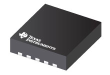
Datasheet Texas Instruments TPS63000DRCT
| Manufacturer | Texas Instruments |
| Series | TPS63000 |
| Part Number | TPS63000DRCT |

96% Buck-Boost Converter with 1.8A Current Switches in 3x3 QFN 10-VSON -40 to 85
Datasheets
TPS6300x High-Efficient Single Inductor Buck-Boost Converter With 1.8-A Switches datasheet
PDF, 1.1 Mb, Revision: C, File published: Oct 30, 2015
Extract from the document
Prices
Status
| Lifecycle Status | Active (Recommended for new designs) |
| Manufacture's Sample Availability | Yes |
Packaging
| Pin | 10 |
| Package Type | DRC |
| Industry STD Term | VSON |
| JEDEC Code | S-PDSO-N |
| Package QTY | 250 |
| Carrier | SMALL T&R |
| Device Marking | BPT |
| Width (mm) | 3 |
| Length (mm) | 3 |
| Thickness (mm) | .9 |
| Pitch (mm) | .5 |
| Max Height (mm) | 1 |
| Mechanical Data | Download |
Parametrics
| Duty Cycle(Max) | 100 % |
| Iout(Max) | 0.8 A |
| Iq(Typ) | 0.04 mA |
| Operating Temperature Range | -40 to 85 C |
| Package Group | VSON |
| Rating | Catalog |
| Special Features | Enable,Frequency Synchronization,Light Load Efficiency,Load Disconnect,Synchronous Rectification,UVLO Fixed |
| Switch Current Limit(Min) | 1.2 A |
| Switch Current Limit(Typ) | 1.8 A |
| Switching Frequency(Max) | 1500 kHz |
| Switching Frequency(Min) | 1250 kHz |
| Topology | Buck/Boost |
| Type | Converter |
| Vin(Max) | 5.5 V |
| Vin(Min) | 1.8 V |
| Vout(Max) | 5.5 V |
| Vout(Min) | 1.2 V |
Eco Plan
| RoHS | Compliant |
Design Kits & Evaluation Modules
- Evaluation Modules & Boards: TPS63000EVM-148
TPS63000 5.5V Input, 3.3V Output, 1A Buck-Boost Converter Evaluation Module Board
Lifecycle Status: Active (Recommended for new designs)
Application Notes
- Dynamically Adjustable Output Using the TPS63000PDF, 188 Kb, File published: Aug 15, 2006
This application report provides a schematic and design procedure for implementing a dynamically adjustable output for the TPS63000 using a digital-to-analog converter or other input voltage source. - Fully integrated TPS6300x buck-boost converter extends Li-ion battery lifePDF, 168 Kb, File published: Oct 10, 2006
- Low-power TEC driverPDF, 75 Kb, File published: Nov 18, 2014
TPS63020 Low Power TEC Driver - High Efficiency DCDC Converter Reference Design for Stellaris (Rev. A)PDF, 952 Kb, Revision: A, File published: Apr 7, 2010
- Extending the Soft Start Time in the TPS63010 Buck-Boost ConverterPDF, 262 Kb, File published: Dec 5, 2012
- TMS320DM355 DSP Power Reference Design PR742 (Rev. A)PDF, 199 Kb, Revision: A, File published: Aug 8, 2008
This reference design is for the TMS320DM335/DM355 digital signal processor (DSP) and accounts for voltage, current, and sequencing requirements. The operating input voltage ranges from 2 V to 5.5 V for Li-ion batteries and 3 AA batteries. This design also can work with 2 AA batteries with some limitations. The design is optimized for efficiency over the full range of operation and low overall cos - Basic Calculations of a 4 Switch Buck-Boost Power Stage (Rev. B)PDF, 400 Kb, Revision: B, File published: Jul 9, 2018
This application note gives the equations to calculate the power stage of a non-inverting buck-boost converter built with an IC with integrated switches and operating in continuous conduction mode. See the references at the end of this document if more detail is needed. - Minimizing Ringing at the Switch Node of a Boost ConverterPDF, 201 Kb, File published: Sep 15, 2006
The application report explains how to use proper board layout and/or a snubber to reduce high-frequency ringing at the switch node of a boost converter. - Design considerations for a resistive feedback divider in a DC/DC converterPDF, 393 Kb, File published: Apr 26, 2012
- QFN and SON PCB Attachment (Rev. B)PDF, 821 Kb, Revision: B, File published: Aug 24, 2018
- IQ: What it is what it isn’t and how to use itPDF, 198 Kb, File published: Jun 17, 2011
- Performing Accurate PFM Mode Efficiency Measurements (Rev. A)PDF, 418 Kb, Revision: A, File published: Dec 11, 2018
When performing measurements on DC-DC converters using pulse frequency modulation(PFM)or any power save mode proper care must be taken to ensure that the measurements are accurate. An accurate PFM mode efficiency measurement is critical for systems which require high efficiency at low loads such as in smart home systems tablets wearables and metering. - 1.8V – 5.5V Input, High-Efficiency DCDC Converter Reference Design for MSP430 (Rev. B)PDF, 961 Kb, Revision: B, File published: Jun 14, 2010
This reference design is presented to help application designers and others who are trying to use the MSP430 in a system with an input voltage in the range of 1.8 V to 5.5 V, and who must increase the application run time by making use of the complete battery voltage range while still maintaining high efficiency over the entire battery life.
Model Line
Series: TPS63000 (4)
- TPS63000DRCR TPS63000DRCRG4 TPS63000DRCT TPS63000DRCTG4
Manufacturer's Classification
- Semiconductors > Power Management > Non-isolated DC/DC Switching Regulator > Buck/Boost, Inverting or Split-Rail > Buck/Boost, Inverting or Split-Rail Converter (Integrated Switch)
