Careful device selection and good thermal design practices can help optimize the performance of highly miniaturized dc-dc converters intended for mobile applications.
User demands for high functionality in miniaturized devices such as mobile phones, portable media players, or GPSs oblige designers to use smaller components in each new design. As far as digital ICs are concerned, pursuing Moore’s Law has enabled component manufacturers to substantially reduce chip dimensions and, at the same time, increase performance and integration.
Successive generations of analog ICs also equal or surpass the performance of their predecessors within a smaller printed-circuit board (PCB) footprint. Power semiconductor manufacturers are pursuing miniaturization to enable greater power-handling capabilities within a smaller footprint as well, helping to deliver the highest possible power density.
Pursuing this goal, however, imposes tougher thermal management challenges for system designers. The energy lost during power conversion is released as heat. Reducing the size of the component relative to the quantity of heat produced can lead to higher operating temperatures, simply because the smaller die has less ability to radiate heat. Unwanted effects may include poor reliability, unpredictable device behavior, and, at the extreme, destruction of the device. In general, higher junction temperatures lead to higher failure rates.
Using ultra-miniature power devices successfully in modern portable applications requires careful attention at both the component level and the board level to minimize the quantity of heat generated within the device and to ensure its efficient removal (Fig. 1).To minimize heat generation, device designers prioritize high-power conversion efficiency. For example, switching converters are preferred over linear operation for general-purpose applications such as point-of-load (POL) regulators. The best of these devices can achieve peak efficiencies from 95% to 97%.
 |
|
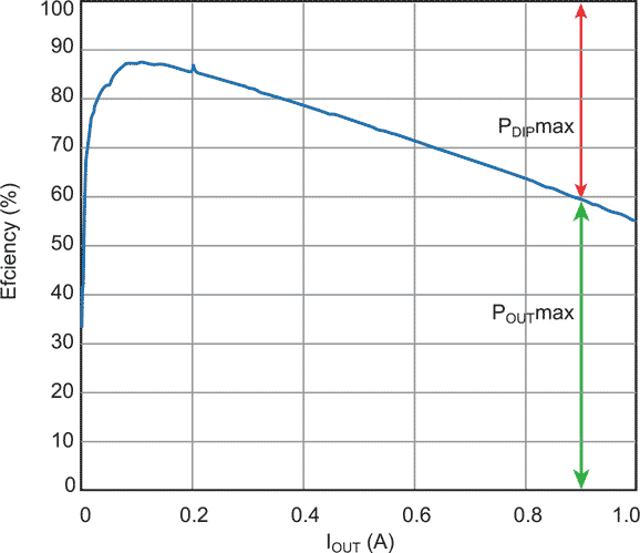
| Figure 1. | Operating efficiency of the NCP1529 versus output current, at an 85°C ambient temperature, 2.7-V input, and 1.2-V output voltage. |
To promote efficient heat removal, several innovative power packages in miniature form factors have recently emerged. They are optimized to minimize thermal resistance between the die and the case, allowing heat to be removed efficiently from the device.
Among the latest packages aimed at portable applications, ultra-miniature leadless types, such as µDFN or µCSP, incorporate an exposed metallic pad on the underside. The pad is soldered down to conduct heat directly into the PCB. Package dimensions can be 2 mm2 or smaller, and devices in such packages can deliver continuous current in the region of 1.5 A max.
To ensure reliable operation and maximum longevity at the highest possible output current when designing with these devices, engineers need to apply sound thermal design principles, taking into account the manufacturer’s recommendations on aspects such as board layout.
Calculating power Dissipation
The power dissipated by a switching converter can be written as:
![]()
Assuming the regulator generates a fixed output voltage, power dissipation is highest at maximum output current and worst-case efficiency. This occurs at high ambient temperature and minimum input voltage. Analyzing the design of a dc-dc converter will demonstrate how to calculate the necessary power dissipation under worst-case conditions and will help to understand how this relates to the package thermal resistance and the maximum permissible ambient operating temperature.
Take, for example, a dc-dc converter such as ON Semiconductor’s NCP1529. Available in a thermally enhanced 2- by 2- by 0.5-mm µDFN-6 or a 3- by 1.5- by 1-mm TSOP5 package, this device is designed for battery-powered devices. An input-voltage range of 2.7 to 5.5 V allows operation from a single-cell lithium-ion (Li-ion) power source or a three-cell alkaline/NiCd/NiMH battery. Output voltage is adjustable from 0.9 to 3.9 V, and maximum output current is 1.0 A.
Furthermore, the IC provides internal thermal shutdown circuitry to prevent catastrophic damage to the device if the maximum junction temperature is exceeded. If the temperature reaches 180°C, the device shuts down, with all power transistors and control circuits turned off. The device will restart in soft-start mode when the temperature falls below 140°C.
Of course, the optimum application design should look to lower the potential for shut-down conditions to occur. One of the first steps in ensuring this is to have a clear understanding of operating efficiency.
Let us consider such a device supplying an IC core voltage of 1.2 V and drawing up to 900 mA. At a 0.9-A output current, the device is operating at 60% efficiency. Substituting these values into Equation 2 produces the following expression for worst-case power dissipation:
![]()
This dissipation is important to help optimize the thermal performance of the application.
Relating power To Temperature
Thermal resistance (RθJA) is the term used to describe the ability of the package to transfer heat from the silicon junction to ambient. The lower the thermal resistance, the better the device can transfer heat. RθJA is expressed in terms of °C/W, and it provides a vehicle for engineers to relate electrical power (dissipated) in watts to temperature in degrees Celsius.
Datasheets for the latest power devices tend to claim very low values for RθJA, but system designers must pay careful attention to the PCB layout and thermal design if they are to achieve the expected performance in the end product. The NCP1529 datasheet shows RθJA for the device alone (220°C/W in µDFN-6 package) and also when used with the recommended board layout (40°C/W). The figures indicate that PCB design has a significant influence on thermal resistance. In fact, following the manufacturer’s recommendations can reduce the effective RθJA by a factor of five.
Knowing both RθJA and PDIP(max), the maximum permissible ambient temperature for the application can be calculated using the following expression:
![]()
where TJmax is the maximum junction temperature allowed (150°C for NCP1529).
| Conversion between electrical and thermal domains | ||
|
Package
|
TSOP-5
|
µDFN-6
|
|
PDIPmax (mW)
|
720
|
720
|
|
RθJA (°C/W)
|
110
|
40
|
|
TAmax (°C/W)
|
70.8
|
121.2
|
Remembering that the NCP1529 is available in TSOP-5 and µDFN-6 packages, the effect of each option on the operating envelope of the application can be quickly assessed. The table summarizes power dissipation, package thermal resistance, and calculated maximum ambient temperature for each case. It also shows that package selection is a key concern if the converter is to operate satisfactorily up to the maximum anticipated ambient temperature.
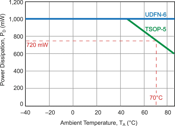
Another way to assess the effect of package thermal characteristics on performance is to inspect the power derating curves. Figure 2 shows the published curves for the NCP1529, detailing the maximum ambient temperature threshold versus power dissipation for the µDFN-6 and TSOP-5 packages.
 |
|
| Figure 2. | Maximum ambient temperature threshold versus power dissipation for the NCP1529 with μDFN-6 and TSOP-5 packages. |
Below 70°C, both packages can dissipate 720 mW and satisfy the worst-case requirement for this application. However, the improved dissipation capabilities of the µDFN-6 package allow a higher maximum temperature than can be sustained by an equivalent converter design based on the TSOP-5 variant. The performance advantage of the µDFN-6 package can be explained by its thermally enhanced structure, featuring an exposed metal pad that significantly reduces the thermal resistance from the die to the application PCB.
Thermal Design guidelines.
In each calculation, the value for TA assumes the best possible thermal resistance; i.e., the thermal resistance achieved when using the recommended board layout. As mentioned previously, board layout can have a profound effect on the thermal performance of the device and, consequently, the application. Designers using any dc-dc converter IC should consult documentation for the chosen part to be sure of achieving the expected performance when the design is implemented in hardware.
Thermal performance can be optimized using features such as thermal dissipation vias, maximizing key trace widths, making thermal connections to ground or power planes, or specifying a thermally enhanced PCB material, such as an insulated metal substrate. The thermal layout guidelines for the NCP1529 recommend enlarging the VIN trace and adding several vias to create multiple thermal connections to the power plane.
In addition, it is recommended to connect the regulator’s ground pin to the PCB top plane. The top, bottom, and ground planes should be connected using free vias to increase the effective size of the radiator, and these should be located as close as possible—underneath is ideal—to the exposed pad when using the µDFN-6 package. The µDFN-6 exposed pad must be correctly soldered to the main radiator of the PCB.
Of course, the designer must also bear in mind the effect of board layout on the electrical performance of the converter. Optimum thermal layout should complement features such as large traces for high-current paths, as well as separate power and ground planes, which help to maximize noise immunity and loop stability of the regulator.
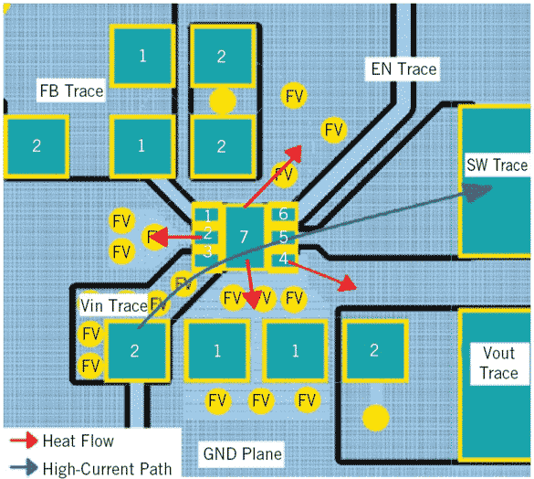
Figure 3 shows the recommended pad layout when using the NCP1529 in µDFN-6 package, accounting for electrical and thermal considerations. The red arrows indicate the flow of thermal energy from the package toward ambient.
 |
|
| Figure 3. | Recommended pad layout for the NCP1529 in a µDFN-6 package, accounting for electrical and thermal considerations. |
To implement high-performance dc-dc converters within the exacting space constraints of today’s mobile products, designers must pay careful attention to operating conditions, power dissipation, component performance, and thermal design. The latest smalloutline package technologies with enhanced thermal features allow higher dissipation than more established power packages. Using these in combination with best-practice thermal design at the board level allows designers of portable systems to achieve reliable high current designs within compact dimensions.
