Umesh Jayamohan, Analog Devices
Analog Dialogue
Introduction
The design of the input, or front end, of any high-performance analog-to-digital converter (ADC), especially an RF-sampling ADC, is critical to achieving the desired system-level performance. In many cases, the RF-sampling ADC digitizes a signal bandwidth of hundreds of megahertz. The front end can be active (using an amplifier) or passive (using transformers or baluns) depending on the system’s requirements. In either case, the components must be carefully chosen to provide optimum ADC performance in the frequency band of interest.
RF-sampling ADCs are fabricated using deep submicron CMOS process technology, and the physics of semiconductor devices tells us that smaller transistor geometries support lower maximum voltages. Hence, the data sheet specifies the absolute maximum voltages that should not be exceeded due to reliability reasons. Comparing data sheets from older devices with those of state-of-the-art RF-sampling ADCs demonstrates this decrease in voltage.
In receiver applications where the ADC digitizes the input signal, systems designers must pay careful attention to the absolute maximum input voltage. This parameter directly affects the ADC’s lifetime performance and reliability. An unreliable ADC would render the entire radio system useless, and the cost of replacing it could be substantial.
To counter the risk from overvoltage stress, RF-sampling ADCs include circuitry that detects high thresholds, allowing the receiver to compensate by adjusting the gain with an automatic-gain-control (AGC) loop. With a pipelined ADC, however, the inherent latency associated with the architecture can briefly expose the input to a high level, potentially harming the ADC inputs. This article discusses a simple method that can augment the AGC loop to protect the ADC.
Input Architectures
RF-sampling ADCs are implemented with several different designs, the most common being the pipelined architecture, which cascades several stages to convert the analog signal to digital. The first stage, which is the most critical, can be buffered or unbuffered. The choice of which to use depends on design requirements and performance targets. For example, a buffered ADC usually offers better SFDR across frequency but consumes more power than an unbuffered ADC.
 |
|
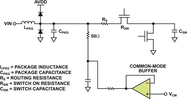
| Figure 1. | Equivalent circuit of an unbuffered RF-sampling ADC input. |
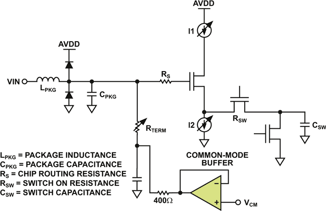
The front-end design will also change according to whether the ADC is buffered or unbuffered. The additional series resistance needed for unbuffered ADCs to handle the input charge kickback would also improve SFDR performance. Figure 1 and Figure 2 show simplified equivalent input circuits of the AD9625 unbuffered and AD9680 buffered RF-sampling ADCs. Only the single-ended inputs are shown for simplicity.
 |
|
| Figure 2. | Equivalent circuit of a buffered RF-sampling ADC input. |
Regardless of the architecture, the absolute maximum voltage sustainable at the inputs of the ADC is governed by the voltages the MOSFETs can handle. The buffered input is more complex and burns more power than the unbuffered input. ADCs employ several different kinds of buffers, the most common of which is a source follower.
Failure Mechanisms
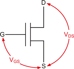
The failure mechanism will differ for buffered and unbuffered ADCs, but failure usually occurs when the maximum allowable gate-source voltage (VGS) or drain-source voltage (VDS) is exceeded. These voltages are illustrated in Figure 3.
 |
|
| Figure 3. | Critical voltages for MOS transistor. |
For example, if VDS exceeds the maximum allowable voltage, it causes a VDS breakdown failure, which usually occurs when the MOSFET is in the off state and an excessive voltage is applied to the drain with respect to the source. If VGS exceeds the maximum allowable voltage, it causes a VGS punch through, also known as oxide breakdown. This usually happens when the MOSFET is on and an excessive voltage is applied to the gate with respect to the source.
Failure Mechanism in an Unbuffered ADC
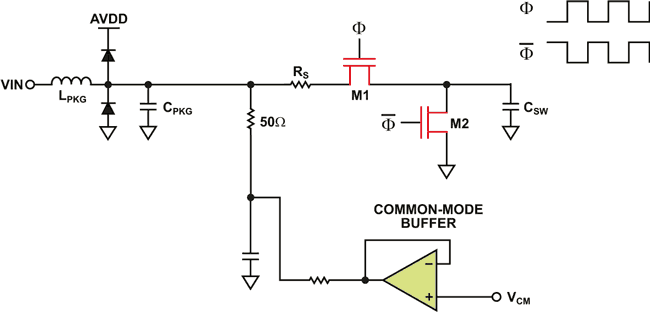
Figure 4 shows an unbuffered ADC input. The sampling process is controlled by out-of-phase clock signals Φ and Ф, which are the sample/hold signal for MOSFET M1 and the reset signal for MOSFET M2. When M1 is on, M2 is off, and capacitor CSW tracks the signal (sample or track mode). When M1 is off, M2 turns on after the comparators in the MDAC have made a decision, resetting the capacitor CSW. This prepares the sampling capacitor for the next sample during the sampling phase. This circuit normally works like a well-oiled machine.
 |
|
| Figure 4. | Failure mode in an unbuffered ADC input. |
High-voltage inputs, however, expose the circuit to stresses that violate the drain-source voltage limit for M2. When a high-voltage input is sampled (M1 is on, M2 is off), M2 is exposed to a large VDS. M2 is off for less than one-half cycle of the sampling clock, but even this transient exposure can deteriorate the reliability of the circuit and render the ADC useless over time. M1 is exposed to a large VDS when in reset mode (M1 off, M2 on), as the input signal is present on its drain.
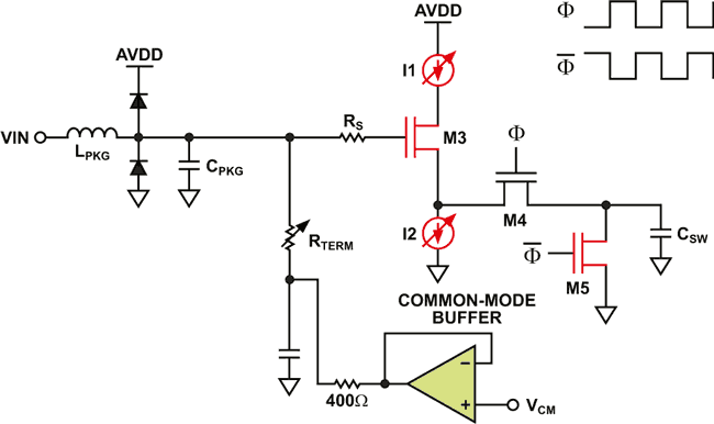
Failure Mechanism in a Buffered ADC
Figure 5 shows a buffered ADC input. The same clock scheme applies for the sampling and reset signals. Regardless of the phase, when the gate of Buffer M3 is exposed to a high-voltage input, it stresses the circuitry that creates currents I1 and I2. Current Source I1 is implemented with a PMOS transistor, whereas I2 is implemented with an NMOS transistor. A high voltage at the gate of M3 causes excessive VDS on both I1 and I2 MOSFETs. In addition, a high voltage on the gate of M3 can result in oxide breakdown (punch through).
 |
|
| Figure 5. | Failure mode in a buffered ADC input. |
The breakdown mechanisms are different for buffered and unbuffered ADCs, so the absolute maximum input voltage also differs as shown in Table 1.
| Table 1. | Absolute Maximum Specifications for Buffered and Unbuffered ADCs | ||||||||||||||||||||||||||||||
|
|||||||||||||||||||||||||||||||
ADC Input Protection Using a TVS Diode
ADC inputs can be protected against high voltages in several ways. Some ADCs, including RF-sampling ADCs in particular, have built-in circuitry that detects and reports when programmed thresholds have been crossed. This fast detect output has some latency, as specified in the data sheet, so it still leaves the ADC inputs exposed for a short time.
The excess voltage can be limited by transient-voltage-stabilizer (TVS) diodes, but they compromise ADC performance during normal operation. Figure 6 shows a circuit that uses TVS diodes to protect against overvoltage conditions.
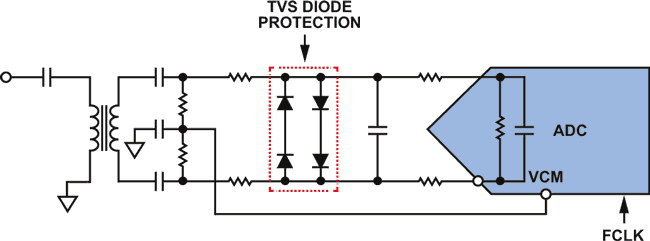 |
|
| Figure 6. | ADC front-end circuit with TVS diode protection. |
Although the TVS diodes protect the ADC inputs by clamping the excess voltage, they severely degrade the harmonic performance. Figure 7 shows a comparison FFT of a 14-bit, 250-MSPS bufferless ADC with a 30-MHz, –1 dBFS input with and without the TVS diode in the front end.
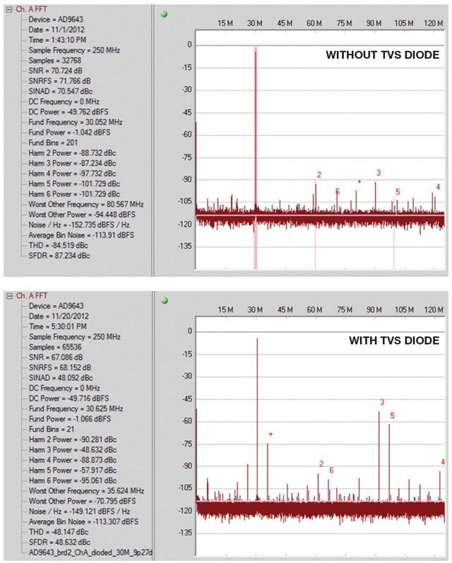 |
|
| Figure 7. | FFT comparison of ADC front-end circuit with and without TVS diode protection. |
The TVS diodes especially degrade the odd harmonics because they act as reverse-biased diodes when not clamping. This PN diode has a junction capacitance, CJ0, that interacts with the nonlinear kickback current generated by the switching action inside the ADC to create a voltage that mixes with the analog input signal. The mixed signal gets sampled inside the ADC and generates a significant third-order harmonic. A time domain plot of the overvoltage condition (Figure 8) shows the clipping action of the TVS diodes. This doesn’t mean that the TVS diode is unsuitable for ADC input protection, but only that the diode specifications must be carefully considered so as to obtain the required performance. A more thorough look is needed in selecting the type of diode and its parameters.
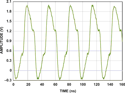 |
|
| Figure 8. | Clipped signal due to TVS diode protection in front-end circuit. |
Protection of RF Sampling ADC Inputs Using Schottky Diodes
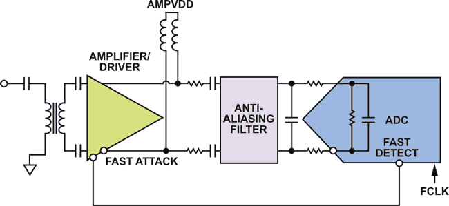
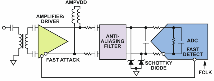
As bandwidths and sample rates have hit the GHz and GSPS range, RF-sampling ADCs simplify radio receiver designs because they do not require as many mixing stages in front of the ADC, but this leaves the ADC inputs vulnerable to overvoltage stresses. Figure 9 shows a typical amplifier driven front-end design for an RF-sampling ADC. The new generation of amplifiers specifically designed to interface with these ADCs have a fast-attack input, which can be configured via the serial peripheral interface (SPI) to attenuate the outputs to a predetermined gain. The fast-attack pin can be configured to respond to the fast-detect output from the RF-sampling ADC. The ADA4961 is an example of the new generation of amplifiers with the fast-attack feature. The AD9680 and AD9625 are examples of RF-sampling ADCs that have the fast-detect feature.
The topology of Figure 9 is good as long as the input voltages are within range. If, for example, this receiver path is exposed to a sudden burst of high voltage at the input, the outputs are going to rise to the voltage of the amplifier’s supply rail (5 V, in this case). This presents a huge swing in excess of the absolute maximum-rated voltage at the inputs of the ADC. The fast detect has some latency (28 clock cycles or 28 ns for the AD9680-1000), so by the time the fast-detect logic output tells the amplifier to assert a fast attack, the ADC has already been exposed to the high voltage for a few clock cycles. This might degrade the ADC’s reliability, so system designs that can’t tolerate this risk will need a secondary mode of protection. A fast-acting Schottky diode with very low device and parasitic capacitance is useful in these situations. Key parameters for specifying the diode can be found in the data sheet.
 |
|
| Figure 9. | Amplifier with fast attack driving RF-sampling ADC with fast detect. |
Reverse breakdown voltage (VBR) – the maximum input voltage at the AD9680 input pins – is about 3.2 V relative to AGND, so a reverse breakdown voltage of 3 V is chosen for the diode.
Junction capacitance (CJ0) – the diode capacitance should be as low as possible to ensure that the diode does not affect the ADC’s ac performance (SNR/SFDR) during normal operation.
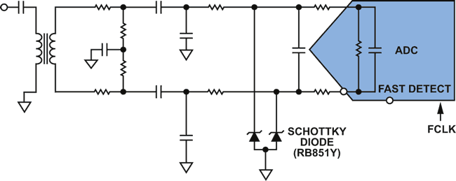
Figure 10 shows a passive front end with a Schottky diode inserted in front of the ADC. The passive front end makes it easy to demonstrate that the Schottky diode can protect the ADC inputs without compromising the ac performance.
 |
|
| Figure 10. | Passive front-end circuit showing RF-sampling ADC and Schottky diode. |
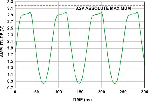
The RF-sampling ADC was tested to input frequencies up to 2 GHz, so an RF Schottky diode was chosen (RB851Y). Table 2 shows the key parameters of the RB851Y that make it suitable for the application. Tests were conducted to show that the diodes prevented the ADC inputs from exceeding the absolute maximum voltage rating of 3.2 V with respect to AGND.
 |
|
| Figure 11. | Single-ended ADC input being clipped by the Schottky diode. |
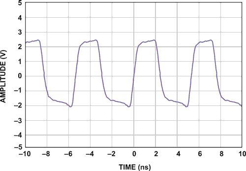
Figure 11 shows a single-ended input (VIN+ pin of the ADC) exposed to a high voltage at 185 MHz. The Schottky diode clamps the voltage to around 3.0 V relative to AGND, preventing the ADC inputs from reaching the 3.2-V limit. Figure 12 shows a differential signal at the input of the AD9680 being clipped by the Schottky diodes.
| Table 2. | Key Parameters for the Schottky Diode Used to Protect RF-Sampling ADC Inputs |
||||||||||||
|
|||||||||||||
Next, we measured performance during normal operation. The AD9680 was controlled as per data sheet recommendations, but the inputs were modified as shown in Figure 10. The analog input frequency was varied from 10 MHz to 2 GHz. The ultralow value of CJ0 should not impact the ADC’s SNR and SFDR performance.
 |
|
| Figure 12. | AD9680 differential inputs clipped by Schottky diodes. |
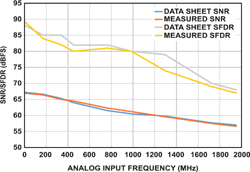
The Schottky diodes do not affect the SNR at all, but the SFDR deviates from the expected value at some frequencies, as shown in Figure 13. This may be caused by a mismatch in the differential signal or kickback from the ADC. The evaluation board is designed for a wide band, from dc to 2 GHz, so while it does a good job overall across the entire band, some components may interact with the Schottky diodes at certain frequencies.
 |
|
| Figure 13. | SNR/SFDR vs. analog input frequency for AD9680 with Schottky diode protection. |
Most applications do not use the entire 2-GHz band, so it is possible to tune the front end to the required signal bandwidth of interest by modifying the input for overvoltage protection. Careful selection of the Schottky diode can protect the ADC inputs, allowing a system designer to implement an amplifier driven front-end circuit using the latest fast-attack and fast-detect features, as shown in Figure 14.
 |
|
| Figure 14. | ADA4961 driving the AD9680 showing RF-sampling ADC and Schottky diodes. |
Conclusion
This article demonstrated the use of a Schottky diode to protect the inputs of an RF-sampling ADC against overvoltage stresses. Careful scrutiny of the diode’s data sheet is key. A plan to accommodate this circuitry is required to achieve optimal performance in the band of interest. The fast-detect output of an RF-sampling ADC can communicate with the fast-attack input of the latest amplifiers to set the automatic gain control loop.
