By Bonnie Baker
EDN Europe
Surprise, surprise. The bandwidth of an amplifier in a gain of +1 V/V is not the same as the bandwidth of the same amplifier in a gain of –1 V/V. After more than five years of working every day with amplifiers for an industry analogue leader, this was a total surprise to me.
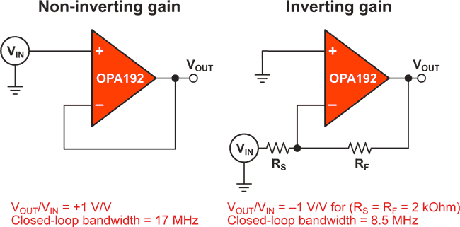
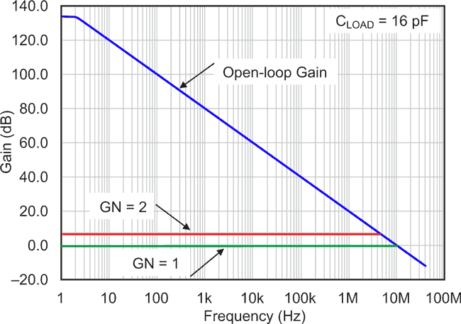
In Figure 1, notice that the closed-loop bandwidth of the noninverting gain circuit in a gain of +1 V/V is 17 MHz, and the inverting gain circuit in a gain of –1 V/V has a 8.5 MHz bandwidth. The definition of noise gain (GN) is the gain of a non-inverting amplifier circuit. With that definition, the GN of the non-inverting circuit is +1 V/V, and the GN of the inverting gain circuit is +2 V/V. Figure 2 shows the open loop gain of the amplifier in Figure 1.
 |
|
| Figure 1. | The simple non-inverting and inverting gain configurations. |
In Figure 2, the OPA192 {2} open loop gain spans from 1 to 100 MHz. See how the 0 dB crossing (GN = 1 V/V) occurs at 10 MHz. Additionally, the 6 dB crossing (GN = 2 V/V) occurs at 5 MHz.
 |
|
| Figure 2. | Using the OPA192, we have the open loop gain curve (blue), noise gain curve for closed loop gain of 2 (red), and noise gain curve for closed loop gain of 1 (green). |
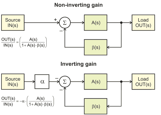
This is a good start if you want to understand these circuits. But let’s go back and look at some control theory. Figure 1 shows a circuit diagram representation of two gain configurations. Figure 3 shows a control theory representation for these two gain configurations.
 |
|
| Figure 3. | Control theory representation of circuits found in Figure 1. |
In Figure 3, alpha (α) is the closed loop inverting gain. A(s) is the open loop gain of the amplifier, or the amplifier’s internal gain. Beta (β(s)) is the feedback factor. In laymen’s terms, it’s the amount of the output that is fed back to the input. For both circuits in Figure 1, beta equals
![]()
Another interesting fact is that 1/beta is equal to the circuit’s GN.
With the non-inverting gain representation in Figure 3, when A(s) is very big the closed loop gain is equal to 1/beta. If you examine the same circuit with A(s) very small or near the 1/beta value, the intersect frequency of the 1/beta curve and A(s) is equal to the gain bandwidth product divided by 1/beta.
The inverting amplifier circuit presents a surprise in this discussion. If A(s) is very big in the Figure 3 inverting gain block diagram, the circuit gain is equal to –R2/R1. If you examine the same circuit with A(s) very small or near the 1/beta value, this occurs at a frequency equal to the gain bandwidth product divided by 1/beta. In this situation, 1/beta is equal to 2.
 |
|
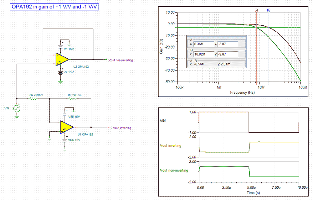
| Figure 4. | TINA-TI circuit configuration with the AC and transient response. The AC curve shows the two signal paths with the inverting bandwidth signal equal to half of the non-inverting signal. |
Don’t take my word for it – give it a try! Run some simulations with TINA-TI and this file {4}. If you have TINA-TI on your computer, you can double click on this line to start your own SPICE simulation. Or better yet, bread board your own circuits to prove or disprove this phenomenon yourself. See the proper circuit configuration in Figure 4.
References
