By Jin-Woo Han & Meyya Meyyappan
IEEE Spectrum
This curious mash-up of vacuum tube and MOSFET could one day replace traditional silicon
 In September 1976, in the midst of the Cold War, Victor Ivanovich Belenko, a disgruntled Soviet pilot, veered off course from a training flight over Siberia in his MiG-25 Foxbat, flew low and fast across the Sea of Japan, and landed the plane at a civilian airport in Hokkaido with just 30 seconds of fuel remaining. His dramatic defection was a boon for U.S. military analysts, who for the first time had an opportunity to examine up close this high-speed Soviet fighter, which they had thought to be one of the world most capable aircraft. What they discovered astonished them.
For one thing, the airframe was more crudely built than those of contemporary U.S. fighters, being made mostly of steel rather than titanium. What’s more, they found the plane’s avionics bays to be filled with equipment based on vacuum tubes rather than transistors. The obvious conclusion, previous fears aside, was that even the Soviet Union’s most cutting-edge technology lagged laughably behind the West’s.
After all, in the United States vacuum tubes had given way to smaller and less power-hungry solid-state devices two decades earlier, not long after William Shockley, John Bardeen, and Walter Brattain cobbled together the first transistor at Bell Laboratories in 1947. By the mid-1970s, the only vacuum tubes you could find in Western electronics were hidden away in certain kinds of specialized equipment – not counting the ubiquitous picture tubes of television sets. Today even those are gone, and outside of a few niches, vacuum tubes are an extinct technology. So it might come as a surprise to learn that some very modest changes to the fabrication techniques now used to build integrated circuits could yet breathe vacuum electronics back to life.
At the NASA Ames Research Center, we’ve been working for the past few years to develop vacuum-channel transistors. Our research is still at an early stage, but the prototypes we’ve constructed show that this novel device holds extraordinary promise. Vacuum-channel transistors could work 10 times as fast as ordinary silicon transistors and may eventually be able to operate at terahertz frequencies, which have long been beyond the reach of any solid-state device. And they are considerably more tolerant of heat and radiation. To understand why, it helps to know a bit about the construction and functioning of good old-fashioned vacuum tubes.
 |
|
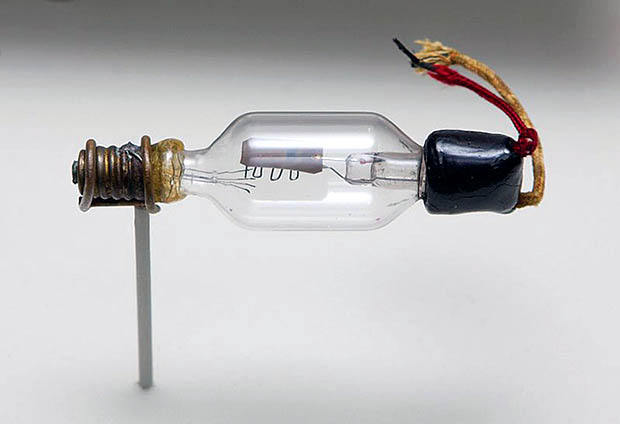
Lightbulb Descendant: |
The thumb-size vacuum tubes that amplified signals in countless radio and television sets during the first half of the 20th century might seem nothing like the metal-oxide semiconductor field-effect transistors (MOSFETs) that regularly dazzle us with their capabilities in today’s digital electronics. But in many ways, they are quite similar. For one, they both are three-terminal devices. The voltage applied to one terminal – the grid for a simple triode vacuum tube and the gate for a MOSFET – controls the amount of current flowing between the other two: from cathode to anode in a vacuum tube and from source to drain in a MOSFET. This ability is what allows each of these devices to function as an amplifier or, if driven hard enough, as a switch.
How electric current flows in a vacuum tube is very different from how it flows in a transistor, though. Vacuum tubes rely on a process called thermionic emission: Heating the cathode causes it to shed electrons into the surrounding vacuum. The current in transistors, on the other hand, comes from the drift and diffusion of electrons (or of «holes» spots where electrons are missing) between the source and the drain through the solid semiconducting material that separates them.
Why did vacuum tubes give way to solid-state electronics so many decades ago? The advantages of semiconductors include lower costs, much smaller size, superior lifetimes, efficiency, ruggedness, reliability, and consistency. Notwithstanding these advantages, when considered purely as a medium for transporting charge, vacuum wins over semiconductors. Electrons propagate freely through the nothingness of a vacuum, whereas they suffer from collisions with the atoms in a solid (a process called crystal-lattice scattering). What’s more, a vacuum isn’t prone to the kind of radiation damage that plagues semiconductors, and it produces less noise and distortion than solid-state materials.
The drawbacks of tubes weren’t so vexing when you just needed a handful of them to run your radio or television set. But they proved really troublesome with more complicated circuits. For example, the 1946 ENIAC computer, which used 17,468 vacuum tubes, consumed 150 kilowatts of power, weighed more than 27 metric tons, and took up almost 200 square meters of floor space. And it kept breaking down all the time, with a tube failing every day or two.
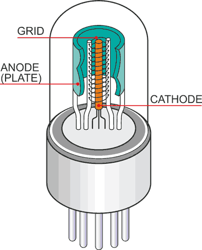 |
| Chip in a Bottle: The simplest vacuum tube capable of amplification is the triode, so named because it contains three electrodes: a cathode, an anode, and a grid. Typically, the structure is cylindrically symmetrical, with the cathode surrounded by the grid and the grid surrounded by the anode. Operation is similar to that of a field-effect transistor, here with the voltage applied to the grid controlling the current flow between the other two electrodes. (Triode tubes often have five pins to accommodate two additional electrical connections for the heated filament.) |
The transistor revolution put an end to such frustrations. But the ensuing sea change in electronics came about not so much because of the intrinsic advantages of semiconductors but because engineers gained the ability to mass-produce and combine transistors in integrated circuits by chemically engraving, or etching, a silicon wafer with the appropriate pattern. As the technology of integrated-circuit fabrication progressed, more and more transistors could be squeezed onto microchips, allowing the circuitry to become more elaborate from one generation to the next. The electronics also became faster without costing any more.
That speed benefit stemmed from the fact that as the transistors became smaller, electrons moving through them had to travel increasingly shorter distances between the source and the drain, allowing each transistor to be turned on and off more quickly. Vacuum tubes, on the other hand, were big and bulky and had to be fabricated individually by mechanical machining. While they were improved over the years, tubes never benefited from anything remotely resembling Moore’s Law.
But after four decades of shrinking transistor dimensions, the oxide layer that insulates the gate electrode of a typical MOSFET is now only a few nanometers thick, and just a few tens of nanometers separate its source and drain. Conventional transistors really can’t get much smaller. Still, the quest for faster and more energy-efficient chips continues. What will the next transistor technology be? Nanowires, carbon nanotubes, and graphene are all being developed intensively. Perhaps one of these approaches will revamp the electronics industry. Or maybe they’ll all fizzle.
We’ve been working to develop yet another candidate to replace the MOSFET, one that researchers have been dabbling with off and on for many years: the vacuum-channel transistor. It’s the result of a marriage between traditional vacuum-tube technology and modern semiconductor-fabrication techniques. This curious hybrid combines the best aspects of vacuum tubes and transistors and can be made as small and as cheap as any solid-state device. Indeed, making them small is what eliminates the well-known drawbacks of vacuum tubes.
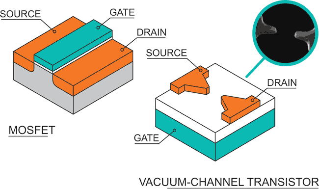 |
| Transistorizing the Vacuum Tube: A vacuum-channel transistor closely resembles an ordinary metal-oxide semiconductor field-effect transistor or MOSFET [left]. In a MOSFET, voltage applied to the gate sets up an electric field in the semiconductor material below. This field in turn draws charge carriers into the channel between the source and drain regions, allowing current to flow. No current flows into the gate, which is insulated from the substrate below it by a thin oxide layer. The vacuum-channel transistor the authors developed [right] similarly uses a thin layer of oxide to insulate the gate from the cathode and anode, which are sharply pointed to intensify the electric field at the tips. |
In a vacuum tube, an electric filament, similar to the filament in an incandescent lightbulb, is used to heat the cathode sufficiently for it to emit electrons. This is why vacuum tubes need time to warm up and why they consume so much power. It’s also why they frequently burn out (often as a result of a minuscule leak in the tube’s glass envelope). But vacuum-channel transistors don’t need a filament or hot cathode. If the device is made small enough, the electric field across it is sufficient to draw electrons from the source by a process known as field emission. Eliminating the power-sapping heating element reduces the area each device takes up on a chip and makes this new kind of transistor energy efficient.
Another weak point of tubes is that they must maintain a high vacuum, typically a thousandth or so of atmospheric pressure, to avoid collisions between electrons and gas molecules. Under such low pressure, the electric field causes positive ions generated from the residual gas in a tube to accelerate and bombard the cathode, creating sharp, nanometer-scale protrusions, which degrade and, ultimately, destroy it.
These long-standing problems of vacuum electronics aren’t insurmountable. What if the distance between cathode and anode were less than the average distance an electron travels before hitting a gas molecule, a distance known as the mean free path? Then you wouldn’t have to worry about collisions between electrons and gas molecules. For example, the mean free path of electrons in air under normal atmospheric pressure is about 200 nanometers, which on the scale of today’s transistors is pretty large. Use helium instead of air and the mean free path goes up to about 1 micrometer. That means an electron traveling across, say, a 100-nm gap bathed in helium would have only about a 10 percent probability of colliding with the gas. Make the gap smaller still and the chance of collision diminishes further.
But even with a low probability of hitting, many electrons are still going to collide with gas molecules. If the impact knocks a bound electron from the gas molecule, it will become a positively charged ion, which means that the electric field will send it flying toward the cathode. Under the bombardment of all those positive ions, cathodes degrade. So you really want to avoid this as much as possible.
Fortunately, if you keep the voltage low, the electrons will never acquire enough energy to ionize helium. So if the dimensions of the vacuum transistor are substantially smaller than the mean free path of electrons (which is not hard to arrange), and the working voltage is low enough (not difficult either), the device can operate just fine at atmospheric pressure. That is, you don’t, in fact, need to maintain any sort of vacuum at all for what is nominally a miniaturized piece of «vacuum» electronics!
But how do you turn this new kind of transistor on and off? With a triode vacuum tube, you control the current flowing through it by varying the voltage applied to the grid – a meshlike electrode situated between the cathode and the anode. Positioning the grid close to the cathode enhances the grid’s electrostatic control, although that close positioning tends to increase the amount of current flowing into the grid. Ideally, no current would ever flow into the grid, because it wastes energy and can even cause the tube to malfunction. But in practice there’s always a little grid current.
To avoid such problems, we control current flow in our vacuum-channel transistor just as it’s done in ordinary MOSFETs, using a gate electrode that has an insulating dielectric material (silicon dioxide) separating it from the current channel. The dielectric insulator transfers the electric field where it’s needed while preventing the flow of current into the gate.
So you see, the vacuum-channel transistor isn’t at all complicated. Indeed, it operates much more simply than any of the transistor varieties that came before it.
Although we are still at an early stage with our research, we believe the recent improvements we’ve made to the vacuum-channel transistor could one day have a huge influence on the electronics industry, particularly for applications where speed is paramount. Our very first effort to fashion a prototype produced a device that could operate at 460 gigahertz – roughly 10 times as fast as the best silicon transistor can manage. This makes the vacuum-channel transistor very promising for operating in what is sometimes known as the terahertz gap, the portion of the electromagnetic spectrum above microwaves and below infrared.
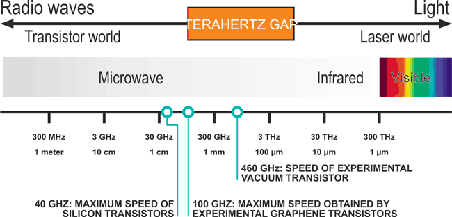 |
| Filling the Gap: Vacuum-channel transistors hold the promise of being able to operate at frequencies above microwaves and below infrared – a region of the spectrum sometimes known as the terahertz gap because of the difficulty that most semiconductor devices have operating at those frequencies. Promising applications for terahertz equipment include directional high-speed communications and hazardous-materials sensing. |
Such frequencies, which run from about 0.1 to 10 terahertz, are useful for sensing hazardous materials and for secure high-speed telecommunications, to give just a couple of possible applications. But terahertz waves are difficult to take advantage of because conventional semiconductors aren’t capable of generating or detecting this radiation. Vacuum transistors could – pardon the expression – fill that void. These transistors might also find their way into future microprocessors, their method of manufacture being completely compatible with conventional CMOS fabrication. But several problems will need to be solved before that can happen.
Our prototype vacuum transistor operates at 10 volts, an order of magnitude higher than modern CMOS chips use. But researchers at the University of Pittsburgh have been able to build vacuum transistors that operate at just 1 or 2 V, albeit with significant compromises in design flexibility. We’re confident we can reduce the voltage requirements of our device to similar levels by shrinking the distance between its anode and cathode. Also, the sharpness of these electrodes determines how much they concentrate the electric field, and the makeup of the cathode material governs how large a field is needed to extract electrons from it. So we might also be able to reduce the voltage needed by designing electrodes with sharper points or a more advantageous chemical composition that lowers the barrier for the electron escaping from the cathode. This will no doubt be something of a balancing act, because changes made to reduce operating voltage could compromise the long-term stability of the electrodes and the resultant lifetime of the transistor.
The next big step for us is to build a large number of vacuum-channel transistors into an integrated circuit. For that, we should be able to use many of the existing computer-aided design tools and simulation software developed for constructing CMOS ICs. Before we attempt this, however, we’ll need to refine our computer models for this new transistor and to work out suitable design rules for wiring lots of them together. And we’ll have to devise proper packaging methods for these 1-atmosphere, helium-filled devices. Most likely, the techniques currently used to package various microelectromechanical sensors, such as accelerometers and gyroscopes, can be applied to vacuum-channel transistors without too much fuss.
Admittedly, a great deal of work remains to be done before we can begin to envision commercial products emerging. But when they eventually do, this new generation of vacuum electronics will surely boast some surprising capabilities. Expect that. Otherwise you might end up feeling a bit like those military analysts who examined that Soviet MiG-25 in Japan back in 1976: Later they realized that its vacuum-based avionics could withstand the electromagnetic pulse from a nuclear blast better than anything the West had in its planes. Only then did they begin to appreciate the value of a little nothingness.
