By Qui Luu, Analog Devices
Analog Dialogue
As more building blocks are added to a radio-frequency integrated circuit (RFIC), more sources of noise coupling arise, making power management increasingly important. This article describes how power-supply noise can affect the performance of RFICs. The ADRF6820 quadrature demodulator with integrated phase-locked loop (PLL) and voltage-controlled oscillator (VCO) is used as an example, but the results are broadly applicable to other high-performance RFICs.
The power-supply noise can degrade linearity by creating mixing products in the demodulator and degrade phase noise in the PLL/VCO. A detailed power evaluation is accompanied by recommended power designs using low-dropout regulators (LDOs) and switching regulators.
With its dual supply and high level of RF integration, the ADRF6820 provides an ideal vehicle for discussion. It uses a similar active mixer core as the ADL5380 quadrature demodulator and the identical PLL/VCO cores as the ADRF6720, so the information presented can be applied to those components. In addition, the power-supply design can be applied to new designs requiring 3.3-V or 5.0-V supplies with similar power consumption.
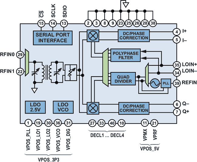
The ADRF6820 quadrature demodulator and synthesizer, shown in Figure 1, is ideally suited for next-generation communication systems. The feature-rich device comprises a high-linearity broadband I/Q demodulator, an integrated fractional-N PLL, and a low-phase-noise multicore VCO. It also integrates a 2:1 RF switch, a tunable RF balun, a programmable RF attenuator, and two LDOs. The highly integrated RFIC is available in a 6-mm × 6-mm LFCSP package.
 |
|
| Figure 1. | ADRF6820 simplified block diagram. |
Power-Supply Sensitivities
The blocks most affected by power-supply noise are the mixer core and the synthesizer. Noise coupled into the mixer core creates unwanted products that degrade linearity and dynamic range. This is especially critical for a quadrature demodulator because the low-frequency mixing products fall within the band of interest. Similarly, power-supply noise can degrade the phase noise of the PLL/VCO. The effect of unwanted mixing products and degraded phase noise are common to most mixers and synthesizers, but the exact level of degradation is determined by the architecture and layout of the chip. Understanding these power-supply sensitivities allows a more robust power design that optimizes performance and efficiency.
Quadrature Demodulator Sensitivities
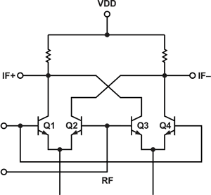
The ADRF6820 uses a double-balanced Gilbert cell active mixer core, as shown in Figure 2. Double-balanced means that both the LO and RF ports are driven differentially.
 |
|
| Figure 2. | Gilbert cell double-balanced active mixer. |
After a filter rejects the high-order harmonics, the resulting mixer outputs are the sum and difference of the RF and LO inputs. The difference term, also called the IF frequency, lies within the band of interest, and is the desired signal. The sum term falls out of band and gets filtered.
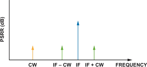
Ideally, only the desired RF and LO signals are presented to the mixer core, but this is rarely the case. Power-supply noise can couple into the mixer inputs and manifest itself as mixing spurs. Depending on the source of the noise coupling, the relative amplitudes of the mixing spurs may vary. Figure 3 shows a sample mixer output spectrum and where the mixing products may reside due to power-supply-noise coupling. In the figure, CW corresponds to a continuous wave or sinusoidal signal that couples on to the power-supply rail. The noise may be the clock noise from a 600-kHz or 1.2-MHz switching regulator, for example. The power-supply noise can cause two different problems – if the noise couples to the mixer outputs, the CW tone will appear at the output with no frequency translation; if the coupling occurs at the mixer inputs, the CW tone will modulate the RF and LO signals, producing products at IF ± CW.
 |
|
| Figure 3. | Sample mixer output spectrum with power-supply noise coupling. |
These mixing products can be close to the desired IF signal, so filtering them out becomes difficult, and dynamic range loss is inevitable. This is especially true for quadrature demodulators because their baseband is complex and centered around dc. The demodulation bandwidth of the ADRF6820 spans from dc to 600 MHz. If a switching regulator with noise at 1.2 MHz powers the mixer core, undesired mixing products will occur at IF ± 1.2 MHz.
Frequency Synthesizer Sensitivities
The references provided at the end of the article offer valuable information on how power-supply noise affects integrated PLL and VCOs. The principles apply to other designs with the same architecture, but nonidentical designs will need their own power evaluation. For example, the integrated LDO on the ADRF6820’s VCO power-supply offers more noise immunity than a PLL power-supply that does not use an integrated LDO.
ADRF6820 Power-Supply Domains and Current Consumption
To design the power-management solution, first examine the RFIC’s power domains to determine which RF blocks are powered by which domain, the power consumption of each domain, the operational modes that affect the power consumption, and the power-supply rejection of each domain. Using this information, sensitivity data for the RFIC can be collected.
The major functional blocks of the ADRF6820 each have their own power pins. Two domains are powered from the 5-V supply. VPMX powers the mixer core, and VPRF powers the RF front-end and input switches. The remaining domains are powered from the 3.3-V supply. VPOS_DIG powers an integrated LDO, which outputs 2.5 V to power the SPI interface, the PLL’s Σ-Δ modulator, and the synthesizer’s FRAC/INT dividers. VPOS_PLL powers the PLL circuitry, including the reference input frequency (REFIN), phase-frequency detector (PFD), and the charge pump (CP). VPOS_LO1 and VPOS_LO2 power the LO path, including the baseband amplifier and dc bias reference. VPOS_VCO powers another integrated LDO, which outputs 2.8 V to power the multicore VCO. This LDO is important for minimizing the sensitivity to power-supply noise.
The ADRF6820 is configurable in several operational modes. It consumes less than 1.5 mW in normal operational mode with a 2850-MHz LO. Decreasing the bias current reduces both power consumption and performance. Increasing the mixer bias current makes the mixer core more linear and improves IIP3, but degrades the noise figure and increases power consumption. If noise figure is of key importance, the mixer bias current can be reduced, decreasing the noise within the mixer core and reducing power consumption. Similarly, the baseband amplifiers at the output have variable current drive capabilities for low impedance output loads. Low output impedance loads require higher current drive and consume more power. The data sheet provides tables showing power consumption for each of the operational modes.
Measurement Procedure and Results
Noise coupling on the power rail produces undesired tones at CW and IF ± CW. To mimic this noise coupling, apply a CW tone to each power pin and measure the amplitude of the resulting mixing product relative to the input CW tone. Record this measurement as the power-supply rejection in dB. The power-supply rejection varies with frequency, so sweep the CW frequency from 30 kHz to 1 GHz to capture the behavior. The power-supply rejection over the band of interest determines whether filtering is required. The PSRR is calculated as:
- CW PSRR in dB = input CW amplitude (dBm) – measured CW feedthrough at I/Q output (dBm)
- (IF ± CW) PSRR in dB = input CW amplitude (dBm) – measured IF ± CW feedthrough at I/Q output (dBm)
- (IF + CW) in dBm = (IF – CW) dBm, as CW tones modulated around the carrier have equal amplitudes.
Lab Setup
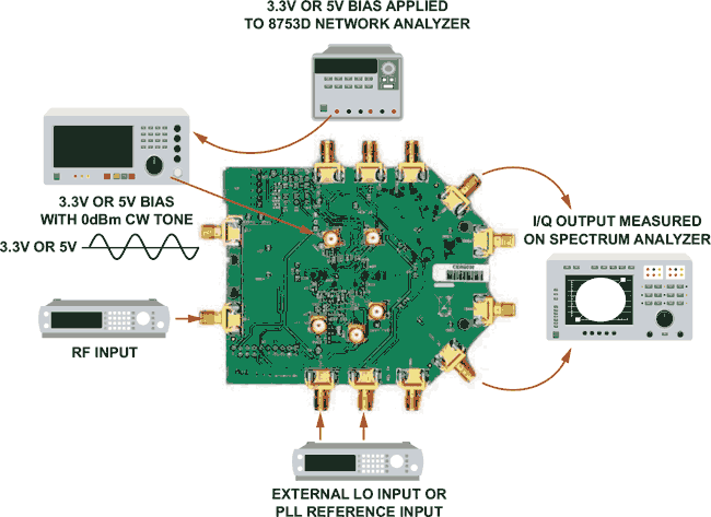
Figure 4 shows the lab setup. Apply a 3.3-V or 5-V dc source to the network analyzer to produce a swept continuous sinusoidal signal with a 3.3-V or 5-V offset. Apply this signal to each of the power rails on the RFIC. Two signal generators provide the RF and LO input signals. Measure the output on a spectrum analyzer.
 |
|
| Figure 4. | ADRF6820 PSRR measurement setup. |
Measurement Procedure
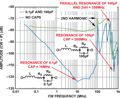
The amplitude of the undesired mixing products depends on the chip’s power-supply rejection, and the size and location of the decoupling capacitors on the evaluation board. Figure 5 shows the amplitude of the (IF + CW) tone at the output given a 0-dB sinusoidal signal on the power pin. With no decoupling capacitors, the amplitude of the undesired tone was between –70 dBc and –80 dBc. The data sheet recommends a 100-pF capacitor adjacent to the device on top of the board and a 0.1-µF capacitor on the back. The resonance of these external decoupling capacitors can be seen in the graph. The transition at 16 MHz is due to the resonance of the 0.1 µF capacitor with a 1-nH parasitic inductance. The transition at 356 MHz is due to the resonance of the 100-pF capacitor with 2 nH of parasitic inductance from both capacitors. The transition at 500 MHz is due to the resonance of the 100-pF capacitor with a 1-nH parasitic inductance.
 |
|
| Figure 5. | Effects of decoupling capacitor resonance on IF ± CW. |
Results
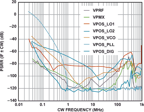
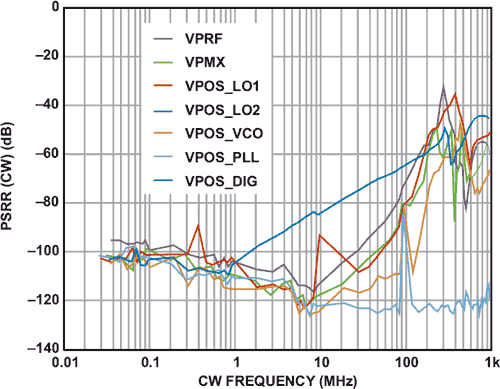
The amplitudes of the interfering signal (CW) on the power-supply rail and the modulated signals (IF ± CW) were measured at the baseband outputs. Noise was introduced to the power rail under test, while the other power supplies remained clean. Figure 6 shows the amplitude of the (IF ± CW) tone when a 0-dB sinusoidal signal was injected on the power pin and swept from 30 kHz to 1 GHz. Figure 7 shows the feedthrough from the CW tone to the baseband outputs.
 |
|
| Figure 6. | PSRR of the (IF ± CW) tone. |
 |
|
| Figure 7. | PSRR of the CW tone. |
References
- Circuit Note CN0147. Powering a Fractional-N Voltage-Controlled Oscillator (VCO) with Low Noise LDO Regulators for Reduced Phase Noise. Analog Devices, Inc., 2010.
- Collins, Ian. Integrated PLLs and VCOs [Part 2]. Radio-Electronics.com, Nov 2010.
