By Qui Luu, Analog Devices
Analog Dialogue
Analysis
The plots provide invaluable data on the supply sensitivities at each power pin. VPOS_PLL has the worst power-supply rejection and is therefore the most sensitive power node. This power pin powers the PLL circuitry, including the reference input frequency, phase-frequency detector, and the charge pump. These sensitive function blocks determine the accuracy and phase performance of the LO signal, so any noise coupled on them propagates directly to the output.
Under the same reasoning, it can be argued that the VCO power-supply is also a critical node. The plots show that VPOS_VCO has much better rejection than VPOS_PLL. This is a result of the internal LDO that actually powers the VCO. The LDO isolates the VCO from noise on the external pin and also provides it with a fixed-noise spectral density. The PLL power supply has no LDO, making it the most sensitive power rail. Thus, isolating it from potential noise coupling is critical for optimal performance.
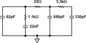
The PLL loop filter attenuates high CW frequencies, so the sensitivity on VPOS_PLL is poor at low frequencies and slowly improves as the frequency sweeps from 30 kHz to 1 GHz. At higher frequencies the amplitude of the interfering tone gets attenuated and the power level injected into the PLL is substantially lower. Thus, VPOS_PLL shows better high-frequency power-supply rejection than the other power domains. The loop filter components were configured for 20 kHz, as shown in Figure 8.
 |
|
| Figure 8. | PLL loop filter configured for a 20-kHz loop bandwidth. |
The power rails, listed from most sensitive to least sensitive, are: VPOS_PLL, VPOS_LO2, VPOS_VCO, VPOS_LO1, VPOS_DIG, VPMX, and VPRF.
Power-Supply Design
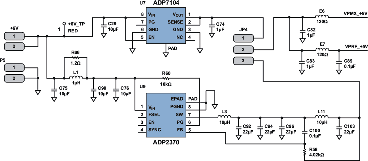
With a good understanding of the maximum power consumption of the ADRF6820 in its various modes and the sensitivity of each power domain, power-management solutions were designed using both switching regulators and LDOs to determine the feasibility of both power solutions. First, a 6-V source was regulated to 5 V and 3.3 V for the ADRF6820 power rails. Figure 9 shows the power design for the 5-V power-supply for VPMX and VPRF. The ADP7104 CMOS LDO can deliver up to 500 mA load current. The ADP2370 low quiescent current step-down (buck) switching regulator can operate at 1.2 MHz or 600 kHz. Additional filtering was added to the switching regulator output to attenuate the switching noise. The ADP2370 can deliver up to 800 mA load current. The ADRF6820’s 5-V rail can be sourced by either the ADP7104 or the ADP2370. Additional decoupling and filtering is applied to each power pin.
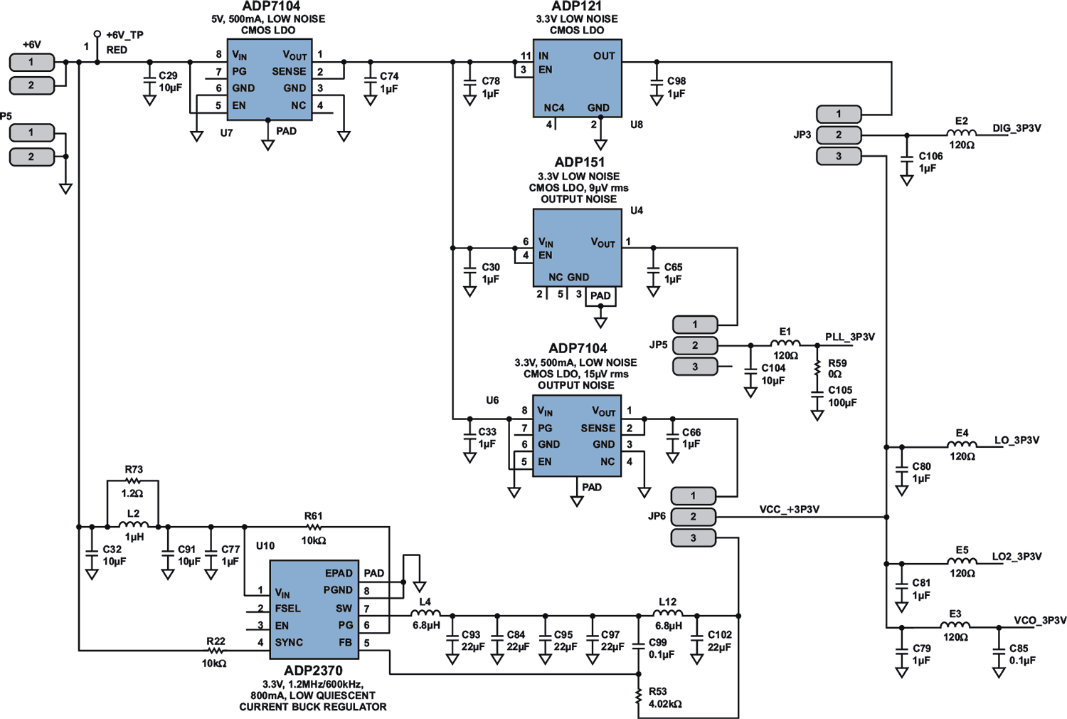
Figure 10 shows the 3.3-V power design. The source voltage is still 6.0 V, but an additional LDO steps the source down to an intermediate voltage before it further gets regulated down to 3.3 V. The extra stage is required to reduce power loss, as a 6-V source regulated directly down to 3.3-V would operate at 55% maximum efficiency. An intermediate stage is not necessary for the switching regulator path because its pulse-width modulation (PWM) architecture minimizes power loss.
 |
|
| Figure 9. | 5-V power design. |
The 3.3-V design allowed for more experimentation. In addition to sourcing the 3.3-V rail with either an LDO or a switching regulator, the VPOS_PLL rail has additional LDO options and the VPOS_DIG rail has an optional isolated LDO. As the PLL power-supply is the most sensitive, three power solutions were tried, each with different output noise: the ADP151 3.3-V ultralow-noise CMOS LDO with 9 µV rms output noise; the ADP7104 3.3-V low-noise CMOS LDO with 15 µV rms output noise; and the ADP2370 3.3-V buck regulator. We want to determine the highest level of power-supply noise that will still maintain the required phase-noise performance. Is the highest performance, lowest noise LDO an absolute necessity?
The ADP121 3.3-V low-noise CMOS LDO was also tried on the VPOS_DIG power rail to determine if digital noise would affect performance. The digital power rail tends to be noisier than the analog supplies due to switching on the SPI interface. We want to determine if the digital 3.3-V power-supply will require its own LDO or if it can be coupled directly to the analog power-supply. The ADP121 was chosen as a low-cost solution.
Conclusions and Power Design Recommendations
 |
|
| Figure 10. | 3.3-V power design. |
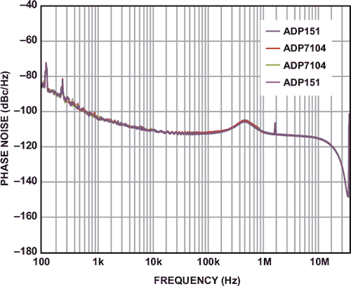
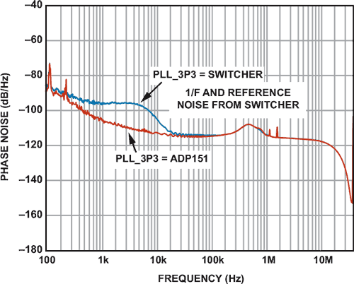
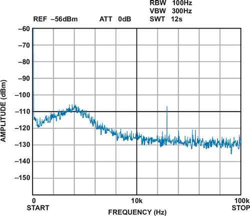
For VPOS_PLL, the most sensitive power-supply rail, the low-cost ADP151 LDO achieves the same phase noise as the ADP7104 high-performance, low-noise LDO, as shown in Figure 11. Performance was degraded when the ADP2370 switching regulator was used, however, as shown in Figure 12. The noise hump is caused by the switching regulator, and can be seen on its output, as shown in Figure 13. Thus, VPOS_PLL can tolerate up to 15 µV rms noise with no degradation in integrated phase noise, but a switching regulator cannot be used to power this pin. No benefit is obtained by using a higher performance, lower noise LDO.
 |
|
| Figure 11. | Integrated phase noise using the ADP151 and ADP7104. |
 |
|
| Figure 12. | Integrated phase noise using the ADP151 and ADP2370. |
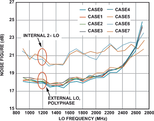
Good phase-noise performance is maintained when either a switching regulator or an LDO powers the remaining supply rails, as shown in Figure 14. The 5-V power-supply pins, VMPX and VPRF, can both be tied together and sourced with a single supply. The 3.3-V power-supply pins, VPOS_LO1, VPOS_LO2, and VPOS_VCO, can also be tied together and sourced by a single supply. VPOS_DIG does not require an independent LDO and can be tied to the analog 3.3-V power-supply.
 |
|
| Figure 13. | Output spectrum of the ADP2370. |
 |
|
| Figure 14. | Switcher vs. LDO noise figure. |
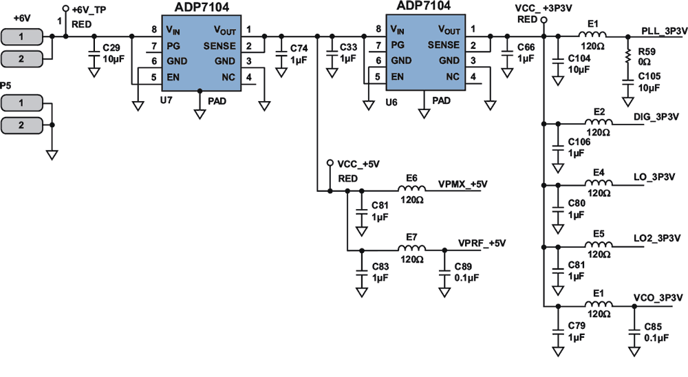
With a 6-V source voltage, the recommended power-supply design, shown in Figure 15, includes the ADP7104 5.0-V and the ADP7104 3.3-V LDOs. This solution uses only LDOs because the source voltage is close to the required supply voltages. The power efficiency is acceptable, so the added cost of filtering components and switching regulators is unnecessary.
 |
|
| Figure 15. | Recommended power-supply design for a 6-V source voltage. |
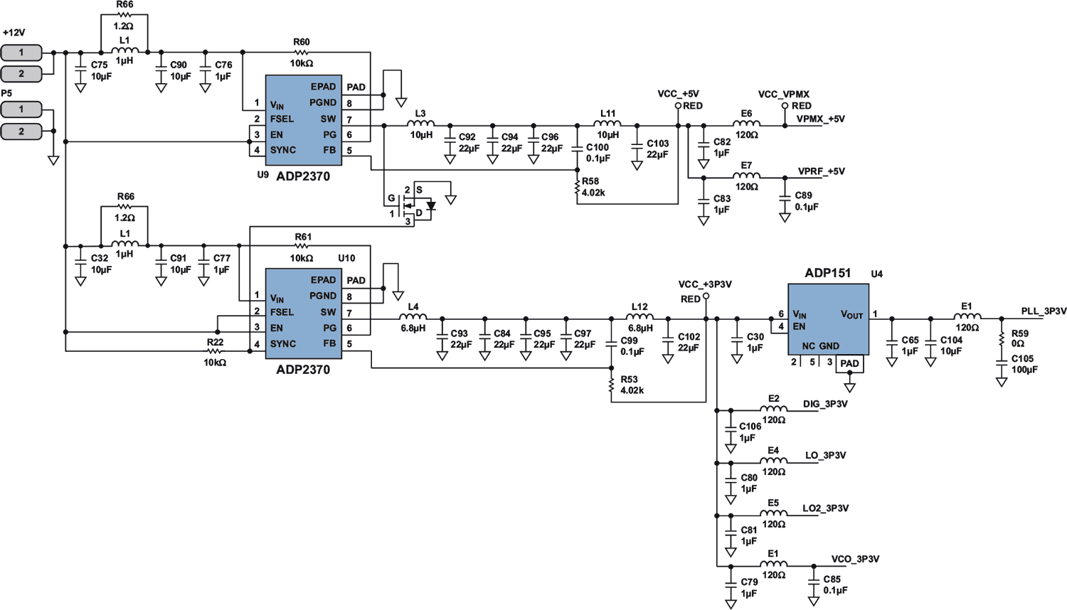
With a 12-V source, the recommended power-supply design, shown in Figure 16, includes two switching regulators and an LDO. The source voltage is much larger than the required supply voltages, so the switching regulators are used to improve power efficiency. All of the power pins except for the sensitive VPOS_PLL supply can be sourced from the switching regulators. Either the ADP7104 or ADP151 can be used for VPOS_PLL.
 |
|
| Figure 16. | Recommended power-supply design for a 12-V source voltage. |
References
1. Circuit Note CN0147. Powering a Fractional-N Voltage-Controlled Oscillator (VCO) with Low Noise LDO Regulators for Reduced Phase Noise. Analog Devices, Inc., 2010.
2. Collins, Ian. Integrated PLLs and VCOs [Part 2]. Radio-Electronics.com, Nov 2010.
