Suzanne Deffree
EDN
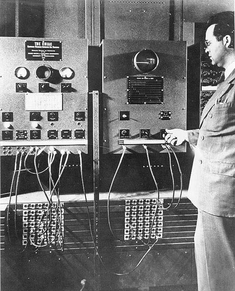
ENIAC (Electronic Numerical Integrator And Computer), the first electronic general-purpose computer, was formally announced on February 15, 1946.
ENIAC had been heavily veiled before its first announcement, although its construction contract had been signed by the United States Army on June 5, 1943.
Code named “Project PX” at the University of Pennsylvania’s Moore School of Electrical Engineering in Philadelphia where it was constructed, the Turing-complete digital computer was capable of being reprogrammed to solve a full range of computing problems and designed to calculate artillery firing tables for the United States Army's Ballistic Research Laboratory, intended for use during World War II.
However, it took approximately one year to design ENIAC, and another 18 months to build, so by the time ENIAC was completed, WWII was over.
By then, others had taken interest in ENIAC and its capabilities would not go to waste. John von Neumann, a mathematician working on the hydrogen bomb at Los Alamos, for example, became aware of this computer. The first test problem run on ENIAC was computation for the hydrogen bomb, not artillery tables, as intended.
 |
|
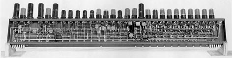
| ENIAC: Accumulator Decade Plug-in Unit. |
ENIAC’s timeline would become important in a legal dispute between Honeywell and Sperry Rand regarding the Atanasoff–Berry Computer (ABC), prototyped in 1939. That dispute lead to patents for the ENIAC being declared invalid.
ENIAC was shut down in November 1946 for a refurbishment and a memory upgrade. It was then transferred to Aberdeen Proving Ground, Maryland, in 1947. On July 29, it was turned on and was in continuous operation until October 2, 1955.
 |
|
| The ENIAC-on-a-Chip. |
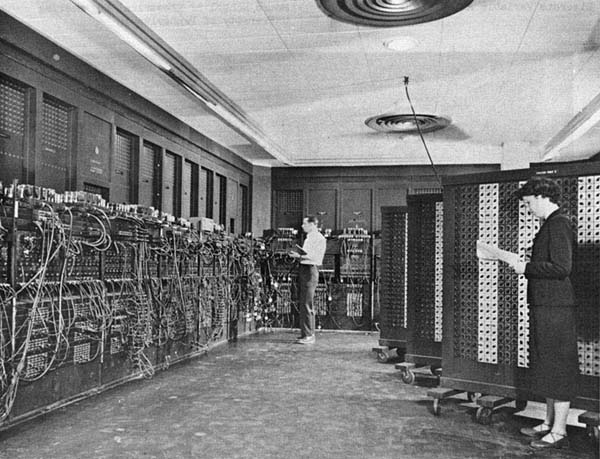
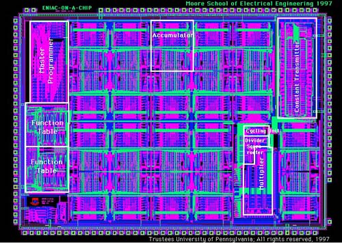
Called the “giant brain,” ENIAC took up an entire room. In the mid 1990s, the Moore School had created “ENIAC-on-a-Chip,” a single 7.44×5.29-mm chip that held all of ENIAC’s functionality.
Parts of ENIAC are now on display at several museums across the globe, including the Smithsonian in Washington, DC, and the Computer History Museum in Mountain View, CA.
