Max Maxfield
EDN
I've been in the electronics and computing industries ever since I graduated with my BSc from Sheffield Hallam University in the UK back in 1980. Since that time, I've designed all sorts of weird and wonderful things (some of which even worked), including my fair share of printed circuit boards (PCBs).
I've also been associated with the Electronic Design Automation (EDA) industry since long before the name EDA was coined. As part of this, I've been involved with all sorts of front-end and back-end design and verification tools for everything from silicon chips to entire systems, including – you guessed it – a variety of PCB layout applications.
Now, anyone who has had anything to do with creating circuit boards will have heard the term "Gerber format." This is an open ASCII vector format for 2D binary images, and it's the de facto standard used by PCB software to describe the printed circuit board images (copper layers, solder mask, legends, etc.). The point is that – as I mentioned in my recent book review [1] – in the 35+ years I've been in the industry, I never thought to question the origin and namesake of this format.
One of the great things about the Embedded Systems Conference (ESC) – in addition to the wide range of highly technical sessions, of course – is the ESC Engineering Theater. This where we showcase all sorts of interesting presentations, such as Jack Ganssle's Mars Ate My Spacecraft, which will debut at the forthcoming ESC Boston, April 13-14, 2016.
Well, I'm delighted to report that another session taking place in the Engineering Theatre at ESC Boston will be David Gerber's The Incredible Story Behind the Gerber PCB File Format. As part of this presentation, David will tell how his father – H. Joseph Gerber – survived the Holocaust to arrive penniless in America where he completed a four-year high school curriculum in just two years and a BSc degree in Aeronautical Engineering in another two.
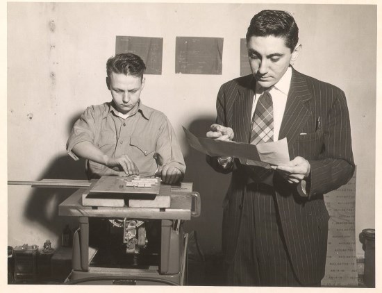 |
| H. Joseph Gerber (right) working with a technician to build one of his early computing devices circa 1950 (Source: The family of H. J. Gerber, Gerber Scientific, Inc., and Ucamco N.V.; Reproduced with permission) |
During his time at university, Joseph turned his pajamas into a revolutionary engineering device, which is now to be found in the Smithsonian National Museum of American History (I tell you – I couldn’t make this stuff up if I tried).
In 1994, Joseph received the U.S. National Medal of Technology for his "Technical leadership in the invention, development, and commercialization of manufacturing automation systems for a wide variety of industries." These industries and products included cars, clothes, engineering, drafting, printing, signs, shoes, billboards, eyeglass lenses, and – of course – printed circuit boards.
All I can say is that I consider this to be a "must-see" session, and you can bet your little cotton socks that I will be arriving at the ESC Engineering Theater early to claim a seat in the front row. Hopefully I'll see you there.
