Applications such as printers, laser-based fiber optic systems, and charged-particle air filtration systems require hundreds or even thousands of volts at low power. Flyback converters and autotransformer boosts are reasonable topology choices, but require custom transformers and require less-than-desirable high-voltage components. A simple boost converter with a voltage multiplier can solve these issues. It uses a standard inductor, low-voltage components, and can provide a large boost ratio in discontinuous mode (DCM).
How does a boost converter with a voltage doubler work?
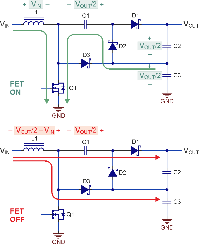
The Figure 1 details the two operating modes of a boost converter with a voltage doubler. The boost converter itself comprises the following components: L1, Q1, D3, and C3. Assume that each output capacitor (C2, C3) is charged to VOUT/2, when the converter is regulating. The green arrows in the top half of this figure show the current paths when the FET is on. This allows the energy transfer capacitor, C1, to charge to a potential of approximately VOUT/2, since diodes D1 and D3 are reverse-biased. During this period, C2 and C3 alone supply current to the load.
 |
||
| Figure 1. | The two operating states of a boost converter with a voltage doubler. |
|
When FET Q1 switches off, the current now follows the paths shown by the red arrows. In the lower path, current flows from the inductor, through D3 to recharge C3 to VOUT/2. Since D3 is conducting, the FET drain voltage is clamped to VOUT/2. Now C1, previously charged to VOUT/2, transfers some of its energy through D1, into C2, recharging it to VOUT/2 also. The sum of C2 and C3 voltages adds up to VOUT. During this period, C2 and C3 are being recharged and the inductor is suppling current to the load.
In this configuration, the boost converter should be designed to supply VOUT/2, but at twice the output current. This circuit configuration reduces the voltage stress on the rectifier diodes, output capacitors, the energy transfer capacitor and FET to VOUT/2 – which is a major benefit. However, the FET and inductor will operate at nearly the same peak current and duty cycle as it would without a doubler, since overall power to the output is unchanged.
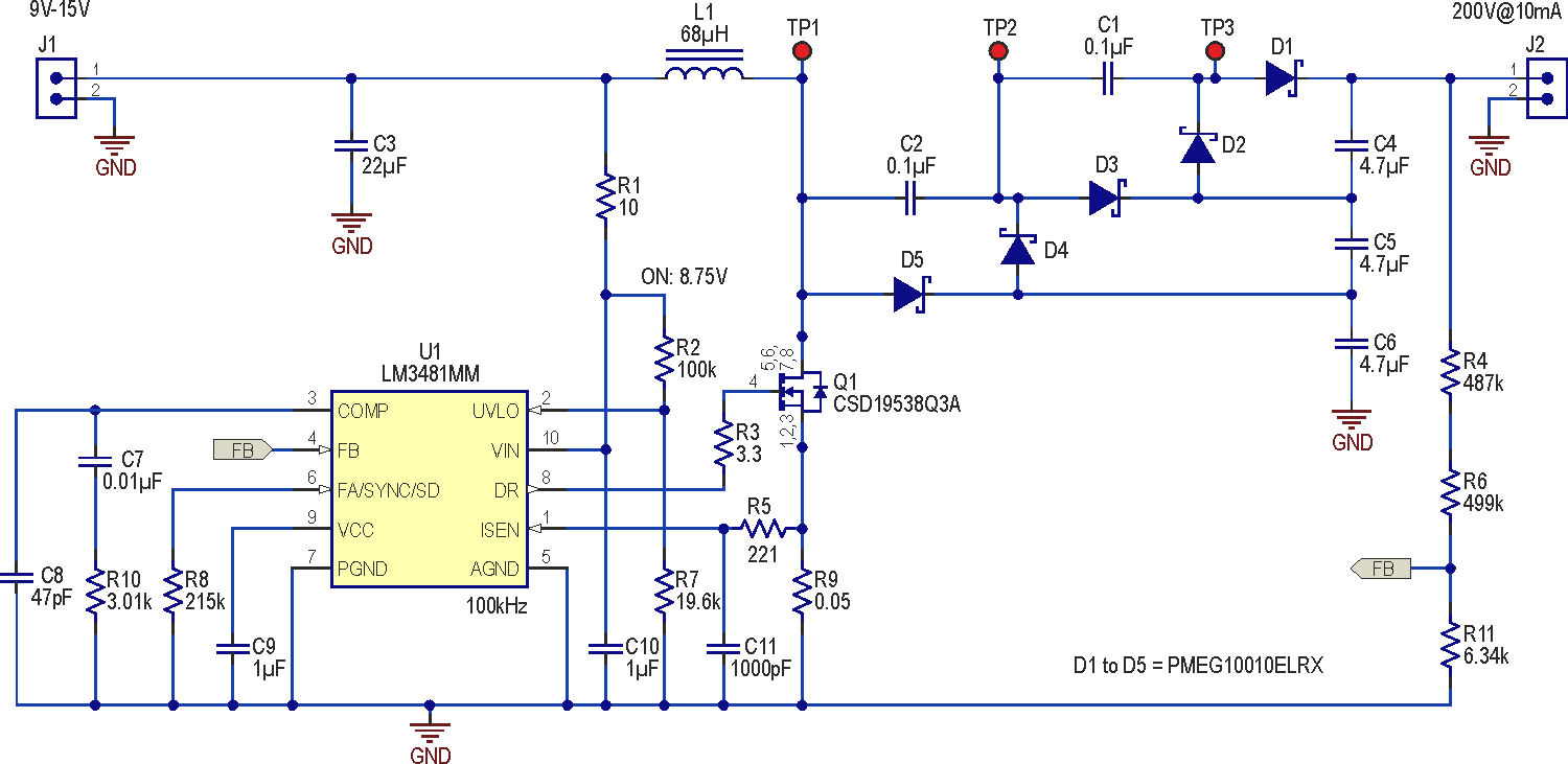
In Figure 2 is an example circuit that takes the doubler stage of Figure 1, and creates a tripler by adding one additional stage. As a multiplier by three times, each power stage component will operate at 33% of the output voltage, or 67 V max for a 200 V output. This allows the use of common 100 V components, providing an adequate 67% derating. The multiplier stages in this circuit can be scaled up as needed to decrease voltage stress further for the same output voltage, or to simply increase the output voltage.
 |
||
| Figure 2. | Boost converter with a voltage tripler reduces component voltage stress. | |
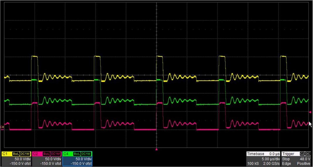
In Figure 3 are the switching waveforms present at TP1, TP2, and TP3 in the example circuit at full load and at 15 V input. As expected, the lower waveform is that of a typical DCM boost converter set to 67 V. The upper two waveforms are identical in shape to the first, but level-shifted by 67 V and 134 V by the multiplier stages. The top waveform (TP3) is then peak-detected by D1 to charge the output capacitors to the 200 V output voltage.
 |
||
| Figure 3. | Switching waveforms of circuit in Figure 2 show the level-shifting action of the multiplier. | |
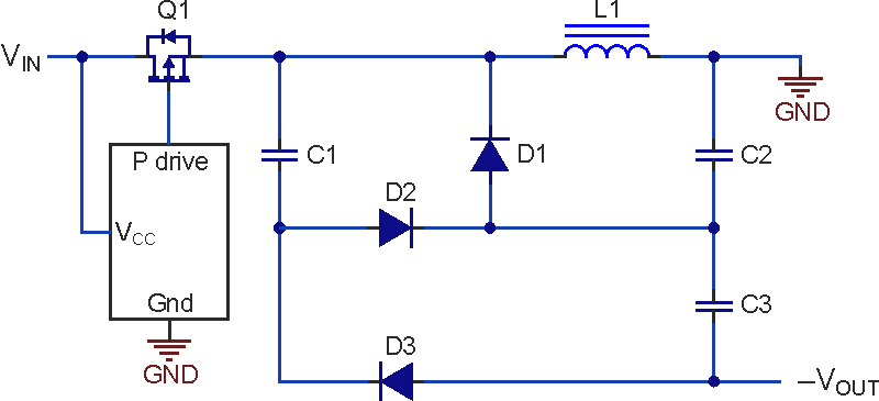
The Figure 4 shows an inverting buck-boost converter with an alternate arrangement of the multiplier components to generate a negative output voltage. Operation is similar to that of Figure 1.
 |
||
| Figure 4. | An inverting buck-boost converter with an alternate arrangement of the multiplier. |
|
When FET Q1 is on, the input voltage is imposed across L1, storing energy, while C1 charges to |VIN+VOUT/2| through D2. The energy transfer capacitor voltage on C1 is higher than that seen on the boost converter. After Q1 turns off, the current in L1 forces D1 to conduct, as in a standard inverting buck-boost, pulling D1’s cathode voltage to –VOUT/2. On that transition, D3 conducts, transferring charge stored in C1 into C3. While the voltages on C2 and C3 are not equal, they are different by the magnitude of the input voltage. So for low-input to high-output voltage ratios, this difference is usually insignificant.
In this application, a P-channel FET is a good choice because the controller used only needs to be rated for the maximum input voltage, since it is ground referenced. A connection to the switching node is not needed when using a P-channel FET. This would be required for an N-channel FET, and since most buck controllers are limited to less than 100 V, this severally limits the negative output voltage. Regardless of the controller used, the sensed negative output voltage must be inverted with an operational amplifier (op amp) to provide a positive feedback voltage for regulation.
