Inexpensive PCB prtotype service ($2 for 10 PCBs prototype)
JLCPCB is a very cheap PCB prototype manufacturer for 10 PCBs 10 × 10 cm double-sided PCBs with a cost of only $2 excluding shipping charges. You can check your own quotes by accessing this link: https://jlcpcb.com.
Step 1: Visit the JLCPCB website
The home page will display a quotation calculator that will then bring you to the actual order page. On the quotation figure, simply enter the size of the PCB, the quantity, the layers, and the thickness.
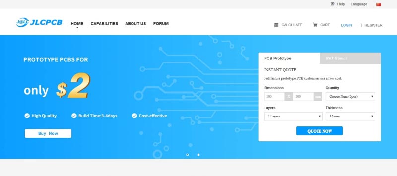
Or you can press the "QUOTE NOW" button to go directly to the order page.
Step 2: Settings on the quote page
After clicking on the "QUOTE NOW" button, you access the page where you can enter all the necessary details.
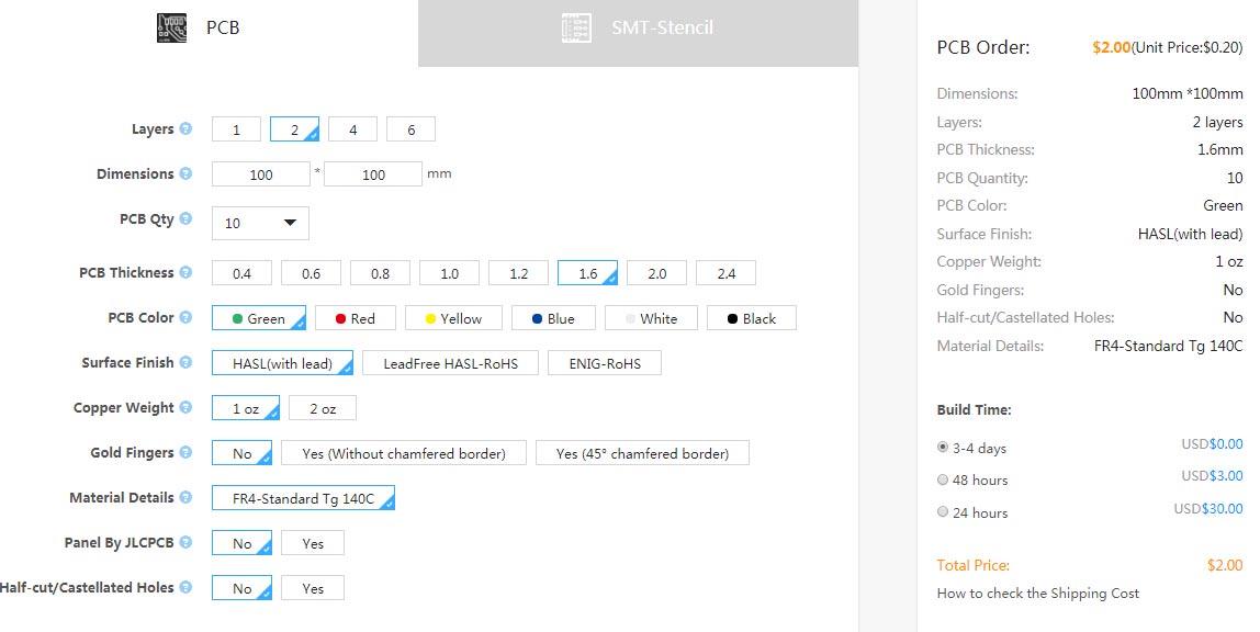
The page already has an excellent default setting for beginners that do not include all technical terms and PCB production standards.
For example, terms such as Surface Finish, Gold Fingers, Material details etc. can be confused by hobbyists, so it is best to avoid changing these settings, leaving the default value.
If, however, you want to know the meaning of these terms you can simply click on the question mark on the side.
In practice, if there are no particular needs, it will be enough to set the size, levels, color, thickness, and quality of PCBs needed. Other default settings can be maintained as they are.
Step 3:
After setting up, click "Save to Cart"
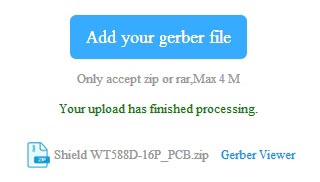
You will see the "Add your gerber file" button that will allow you to add your Gerber files; these will need to be included in a zip or rar file with a maximum size of 4 Mb.
Step 4:
After uploading you will be able to view the Gerber file to make sure that they are correct, to do so click on "Gerber Viewer"
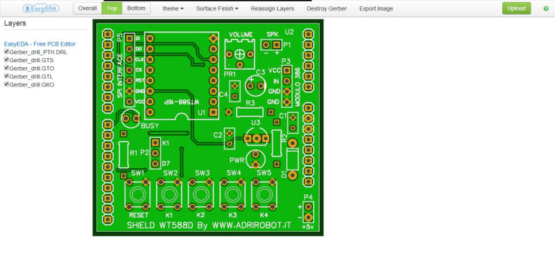
If there is no problem pressing again on "Save to Cart".
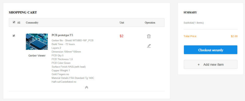
Step 5:
You will then be moved to the carriage page that will show PCB details in order; you can go to the next step by clicking on "Checkout securely"
Step 6:
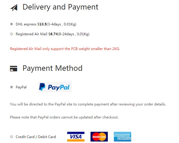
You then enter your master data for the shipment, all fields must be completed. You will then choose the type of shipment that can be by DHL courier or by airmail.
The last step is therefore the payment of PCBs, in this case made through PayPal or credit card.
Quality of PCBs produced by JLCPCB
Examining the boards produced no obvious defects, the copper traces are perfect and the holes are well centered.
After assembling the various components and testing the prototype, this worked perfectly.
 |
 |
| Some projects made. |
Let's see what other strengths are for choosing JLCPCB as the supplier of your PCBs.
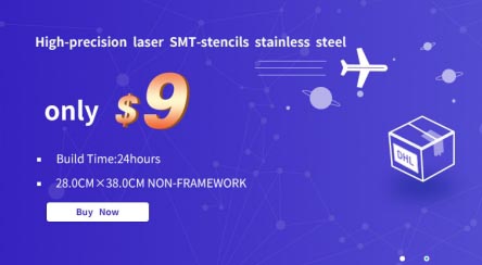
Stencil SMD proposed by JLCPCB
If your electronic boards have SMD components, you may also need the SMD stencil to simplify superficial assembly as it simplifies the application of the soldering paste.
This service is sometimes unavailable to other companies, on JLCPCB this is available at a cost of only $9 for a 38 cm × 28 cm area.
JLCPCB offers a platform for controlling your Gerber – Gerber Viewer.
If you choose, as mentioned above, JLCPCB for the implementation of your project, the program offers online a free Gerber viewer. This way you can use it to control the Gerber PCB files and check how it will be made in different colors, layers and superficial surface. The Gerber viewer can display a very similar image to the actual card.
See for example the following pictures:
 |
 |
|
| Image of Gerber TOP SIDE. | Real picture of PCB product. |
Simplified or non-existent design rules
PCB companies have a set of design rules to which the designer must adhere. If these are not followed, the design could be rejected by the production machine.
По этой причине почти каждая компания, изготавливающая печатные платы, размещает на своем сайте перечень проектных норм, в котором, чаще всего, используются термины, малопонятные новичкам.
For example, a minimum track width is required: 6 mil (0.15 mm), a minimum distance of 6 mil (0.15 mm), minimum vias. The pad: 20 mil (0.5 mm) / hole: 12 mil (0.3 mm).
The JLCPCB site does not require these design details before ordering PCBs. It will simply accept Gerber files. If there is any problem, you will be contacted.
Acceptance of Gerber files created by: Eagle, Altium, Kicad and Diptrace
However, it is not strictly necessary to make their PCBs through EasyEDA, as the PCB manufacturing company should accept Gerber files created by any PCB design software.
However, there are some design rules given by companies that need to be followed. In the case of JLCPCB, 4 tutorials have been published to help users to create their Gerber easily.
There are instructions for: Altium, Eagle, Kicad and Diptrace that are the most popular software for PCB design:
- Altium PCB to gerber files
- Eagle PCB to gerber files
- Kicad PCB to gerber files
- Diptrace PCB to gerber files
For example, here is the movie showing how to export the Gerber file through the EAGLE program.
