Use a TRIAC and optocoupler to automatically change between doubler and bridge configurations
The input-rectifier stage of an offline power supply converts an AC-line voltage to a DC voltage, which powers a DC/DC converter. If you configure the rectifier section as a full-wave bridge for a universal mains input of 92 to 276V rms and 47 to 63 Hz, you must design the DC/DC converter to operate over a wide range of input voltages. This approach increases the cost of components and reduces the efficiency of the dc/dc converter.
For 115V-rms operation, if you configure the rectifier stage as a simple bridge, the output-voltage ripple ranges from 113 to 192V, given a ±20% tolerance on the AC input voltage (Table 1). Note that the voltage ripple corresponds to an effective output capacitance of 165 μF, the series equivalent of two 330-μF capacitors, and to a load of 250W. However, if you configure the rectifier stage as a voltage doubler for 115V-rms operation, the output voltage ranges from 200 to 372V—much closer to the 215 to 387V voltage ripple for 230V-rms operation.
Table 1. 200W input-rectifier/filter section
|
|
115V-rms±20%
60-Hz bridge |
115V-rms±20%
60-Hz doubler |
230V-rms±20%
50-Hz bridge |
|
RMS AC-line voltage
|
92 to 138
|
92 to 138
|
184 to 276
|
|
Peak AC-line voltage
|
130 to 195
|
130 to 195
|
260 to 390
|
|
V1MIN – V1MAX
|
113 to 192
|
200 to 372
|
215 to 387
|
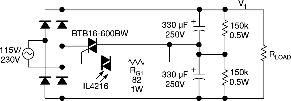
This Design Idea proposes a rectifier stage that automatically configures itself as a voltage doubler for 115V-rms±20% line operation. Figures 1 and 2 show the proposed rectifier stage. The STMicroelectronics snubberless BTB16-600BW TRIAC (triode alternating current) is suitable for a 250W load (Figure 1).
 |
|
| Figure 1. | This AC-rectification circuit uses a TRIAC and an optocoupler to automatically switch between doubler and bridge configurations. |
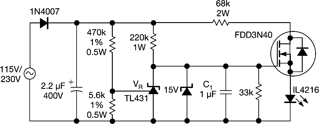
For 115V-rms±20% line operation, the Reference terminal of the TL431 programmable shunt regulator has a voltage lower than its 2.5V internal reference (Figure 2). In this situation, the MOSFET is on, and the IL4216 optocoupler continuously fires the TRIAC.
 |
|
| Figure 2. | This control circuit uses a programmable shunt-regulator IC to sense the AC-input-voltage range. |
For 230V-rms±20% line operation, the Reference terminal has a voltage higher than 2.5V, and the MOSFET and the TRIAC are off. C1 is necessary to prevent the rectifier from starting in doubler mode when you turn on the supply with a low rectified line voltage.
This approach prevents the rectifier stage from changing from doubler mode to bridge mode during start-up, which would create a voltage drop in the bulk output capacitors that would differ from the voltage in steady-state operation. This difference would cause one of the capacitors to have an abnormally high voltage and the other to have an abnormally low voltage.
A practical value of C1 is 1 μF, which introduces an approximately 8-msec time delay for starting in doubler mode. You can use a 15V zener diode to clamp the gate voltage of the MOSFET.