Raju Baddi, Tata Institute of Fundamental Research
EDN
This Design Idea describes a simple way that you can use one hex-inverter package of an unbuffered HD14069UB CMOS (Reference 1) to make four test gadgets:
- a logic probe with well-defined logic-voltage windows and with an input impedance of approximately 1 MΩ;
- a continuity tester whose upper limiting resistance can be tens of ohms to tens of megohms;
- a single or train pulse injector or a modest signal generator; and a high-impedance audio probe.
You can assemble these gadgets using the six inverter gates of a 4069, two or three transistors, and a few passive components.
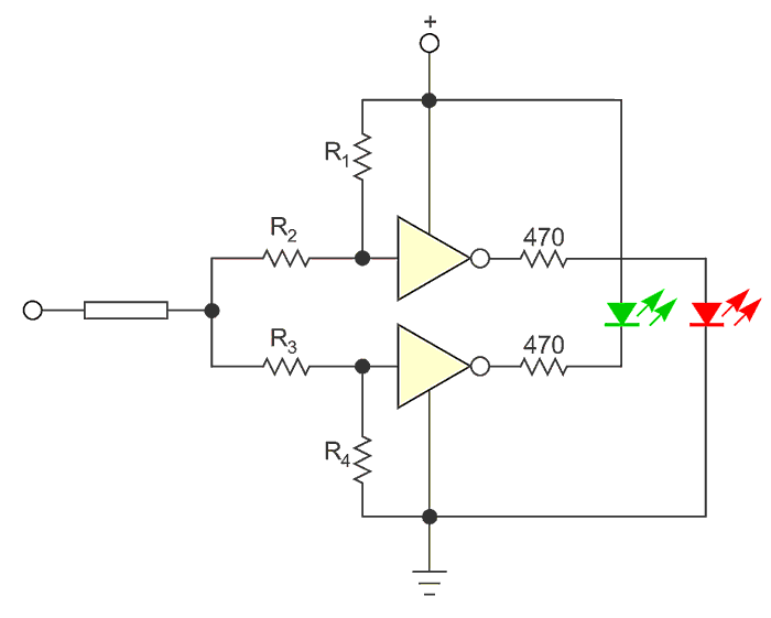
In a two-gate CMOS/TTL-compatible probe, the resistor network comprising R1 through R4 biases the inverter’s inputs (Figure 1). Because of the gates’ high input impedance, R1 through R4 can have values of approximately 100 kΩ to 1 MΩ. The probe’s source/sink current is small at the probe tip because of the high resistances of R1 through R4, as a result, the probe tip essentially does not affect the logic-voltage level at the test point. Knowing the gates’ input threshold voltage, you can calculate the required values of resistors R1 through R4.
 |
|
| Figure 1. | You can make a logic probe TTl/CMOS-compatible using just two gates from a single unit of an HD14069UB hex inverter. The suggested values for threshold and supply voltages are 2.5 and 5V, respectively; those for R1, R2, R3, and R4 are 1 MΩ, 680 kΩ, 200 kΩ, and 1 MΩ, respectively. |
The upper gate detects logic zero, and the lower gate detects logic one. Set an upper limit to the logic-zero voltage and calculate the values of R1 and R2. Arbitrarily select R1=1 MΩ and seek a value for R2 such that the voltage at the input of the upper gate is just the threshold voltage. Thus,
where
- VT is the threshold voltage,
- VL is the logic-zero voltage,
- VS is the supply voltage.
Similarly, set a lower limit on the logic-one voltage VT and seek a value for R4 in terms of R3. By appropriately selecting R3, keeping in mind the quiescent biasing of the gates to keep both the LEDs off in the probe’s suspended condition, you can obtain the value of R4:
The following equation calculates the probe current:
where
- IP is the probe current,
- VI is the probe-tip voltage.
It thus follows that the probe impedance for any voltage at the probe tip is greater than 1 MΩ. For packages of 4069 that exhibit a larger threshold voltage, such as 3 V, you can help reduce it by including a diode followed by a 10-kΩ load resistor to ground in the positive supply rail to the chip.
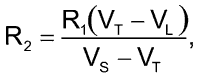
Developers often use continuity testers (Figure 2 and Reference 2) as elementary test gadgets; such testers are indispensable on a work bench. One of the 4069’s gates, with its high input impedance and with a threshold voltage for the transition of the output of the gate, allows you to build the continuity tester with an upper limit on the resistance of the test circuit. The total of the resistance between the probes and the resistance in the switching arrangement forms a voltage-divider network, producing a voltage at the input of the gate. When the two resistances are equal, the voltage at the gate input is half the supply voltage. The transition threshold voltage of the gate is also nearly half the supply voltage; therefore, the selected resistor in the switching branch sets the approximate threshold-continuity resistance.
_en.gif) |
|
| Figure 2. | This single-gate continuity tester has an adjustable detection threshold. |
A useful alternative arrangement is to have a variable resistor in place of the switchable resistors. This approach allows you to set the threshold-continuity resistance arbitrarily by adjusting this resistor after including the desired resistance between the probe tips and observing the LED’s glow. The variable resistor should be set so that the LED just goes off. This method results in a compact arrangement, which a small package can accommodate. Another variable resistor (1 to 2 kΩ) is included in series with the negative probe to make it possible to have a threshold-continuity resistance of approximately 100 Ω or less. You can also use a lower transition threshold voltage for the gate by including a couple of diodes followed by a 10-kΩ load resistor to ground in series with the positive supply rail. This arrangement can also be used to test for live ac-mains lines (Reference 3) with suitable modification, virtually making five gadgets.
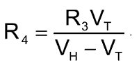
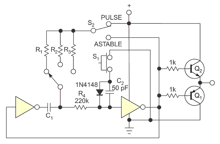
Three gates still remain in the 4069 package; you can use two of them to make an astable oscillator/monostable single-pulse-generator circuit, which a complementary bipolar pair buffers to increase the drive current (Figure 3). You select between a single pulse or a pulse train with an SPDT (single-pole/double-throw) switch set to P (pulse) or A (astable). In pulse mode, pressing the switch produces a brief negative-going pulse at the input to the second gate as C2 begins charging. The resulting high at the gate output causes a positive-going pulse at the junction of Q1 and Q2. It also is latched, and the switch is debounced by the positive feedback through capacitor C1, which begins charging at a time constant that the selection of R1, R2, or R3 determines. When the voltage across C1 equals the threshold voltage, the second gate output returns low, again with positive feedback through C1, driving the second gate input high and ending the pulse.
 |
|
| Figure 3. | A complementary bipolar pair boosts the output current of the oscillator and the single-pulse generator. |
The diode in parallel with C2 is always reverse-biased and serves as a very large-value resistor to discharge C2. Assuming a typical diode leakage of 1 nA, the equivalent resistance at 2.5 V is about 2.5 GΩ. The RC discharge time constant of approximately 125 msec is suitable for the human rate of pushing the button.
The values of R1 through R3 set the astable frequency or the one-shot’s pulse width. The 220-kΩ resistor at the input of the second gate is included to limit the leakage of current from the capacitor into the gate input when its voltage is below that of ground or higher than VDD by 0.6 V. The astable produces a frequency of approximately 1/(2.2RC), whereas the threshold voltage of the gate determines the pulse width of the one-shot, which is approximately 0.7 to 1.1RC.
