Korkut Yegin, Turkey
EDN
Engineers often perceive RF-low-noise-amplifier design as a difficult task. Obtaining a low-noise figure with high stable gain can be challenging – even intimidating. However, with the recent evolution of GaAs (gallium-arsenide) heterojunction FETs, you can design amplifiers with a less-than-1-dB noise figure and high stable gain (Reference 1). This Design Idea describes a low-noise amplifier with a 0.77-dB noise figure.
Manufacturers usually specify low-noise amps’ input/output matching, noise figure, gain, stability, 1-dB compression point, second- and third-order intermodulation products, out-of-band rejection, and reverse isolation. Many of these parameters depend on each other, so it can become complicated to satisfy all of these design criteria in a timely manner (references 2 and 3). Figure 1 shows a flexible amplifier structure that satisfies all of these design criteria.
 |
|
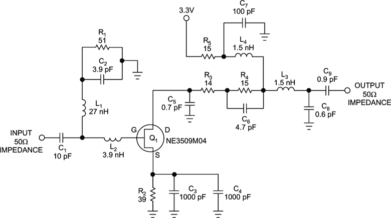
| Figure 1. | You can design a low-noise S-band RF amplifier with a GaAs heterojunction FET. |
The design was created and simulated using Microwave Office AWR. NEC’s NE3509M04 GaAs HJFET (heterojunction field-effect transistor) acts as the low-noise, high-gain transistor. The reactively matched amplifier input provides low noise and high gain using the optimum reflection coefficient value that the data sheet provides. Active biasing and bootstrapping are common design practices for FETs to prevent variations in drain-to-source current especially over temperature. However, this design implements a small, cost-effective, self-biasing circuit that adds no complexity to the circuit. The biasing point for the transistor is a drain-to-source voltage of 2V, and the drain current is 15 mA, at which the transistor produces an acceptable RF gain of approximately 16.5 dB.
Another design goal for the circuit is the unconditional stability of the low-noise amp. Internal feedback of the transistor and excessive gain at the out-of-band frequencies are the primary causes of instability for this type of circuit. The design uses S parameters from the manufacturer to analyze stability. Although the L1, R1, and C2 branch maintains low-frequency dc-to-video-frequency stability for the HJFET, the combination presents as an open circuit to S-band operation and aids in the noise match of the transistor. C5, C8, C9, and L3 primarily achieve the output’s reactive matching and higher frequency stability. Capacitor C6 essentially shorts the bias resistor on the drain line without limiting the maximum stable gain. R3 on the bias line maintains the stability of the amplifier. Shunt capacitor C5 also sinks high-frequency components and harmonics at the drain to ground. The ground vias at the source terminal create a small inductance for inductive degeneration of the amplifier for a good noise match.
 |
|
| Figure 2. |
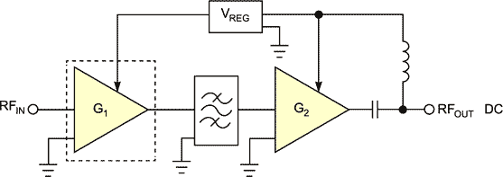
The bandpass filter between two amplifiers rejects out-of-band frequencies. |
Figure 2 shows a two-stage amplifier with a bandpass filter between the amplifier stages. The developers manufactured the design on a standard four-layer, 62-mil-thick FR4 substrate. Unlike cost-effective, two-layer designs, this design uses additional layers for dc routing and passive antenna isolation from high-gain-amplifier stages to prevent any potential signal leakage and feedback that may cause amplifier instabilities. The resulting structure achieves a 0.77-dB noise figure at room temperature, 28.5-dB gain, −16-dBm input power at 1-dB compression, and a −5.8-dBm third-order-intercept point. The output voltage-standing-wave ratio is 1.3-to-1. You can increase the third-order-intercept level by increasing the drain bias current at the expense of an increased noise figure.
 |
|
| Figure 3. |
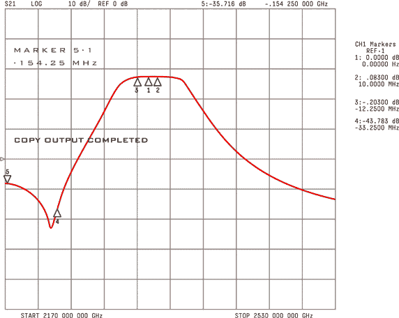
The measured amplifier response has a center frequency of 2.332 GHz. |
Figure 3 shows measured gain performance at −40-dBm input power and −11.5-dBm output power relative to the 2.332-GHz center frequency. The circuit achieves out-of-band rejection with the help of the bandpass filter between the amplifier stages.
References
- Chen, Seng-Woon, “Linearity requirements for digital wireless communications,”Technical Digest of the IEEE 19th Annual Gallium Arsenide Integrated Circuit Symposium, Oct 15 to 17, 1997, pg 29.
- Lee, Thomas H, Planar Microwave Engineering: A Practical Guide to Theory, Measurement, and Circuits, University of Cambridge, 2004, ISBN: 0-521-83526-7.
- “NE3509M04 hetero junction field effect transistor,” California Eastern Laboratories.
