In 1938, the Journal of Scientific Instruments published details of a comparator circuit that converted a slowly varying input signal into an abrupt change in output voltage. Based on cross-coupled thermionic valves, the circuit was developed by American scientist O. H. Schmitt. Since then, the Schmitt trigger has become a staple building block in many signal processing circuits. Hysteresis – the difference between upper and lower voltage thresholds – is inherent in the Schmitt trigger's operation. Provided the input signal crosses both thresholds, the circuit will reject noise contained in the input signal and will produce a rectangular output signal at the same frequency as the input.
Whether you implement a Schmitt trigger using transistors, op amps, or comparators, you need to determine how much hysteresis is required and what the threshold voltages should be. This is usually a simple process if you know the amplitude of the input signal and how much noise it is likely to contain. However, if these parameters are variable or largely unknown, setting the thresholds to produce reliable triggering can be tricky: too much hysteresis can prevent the input signal from crossing one or both thresholds; too little hysteresis can lead to false triggering if the input signal has large noise content.
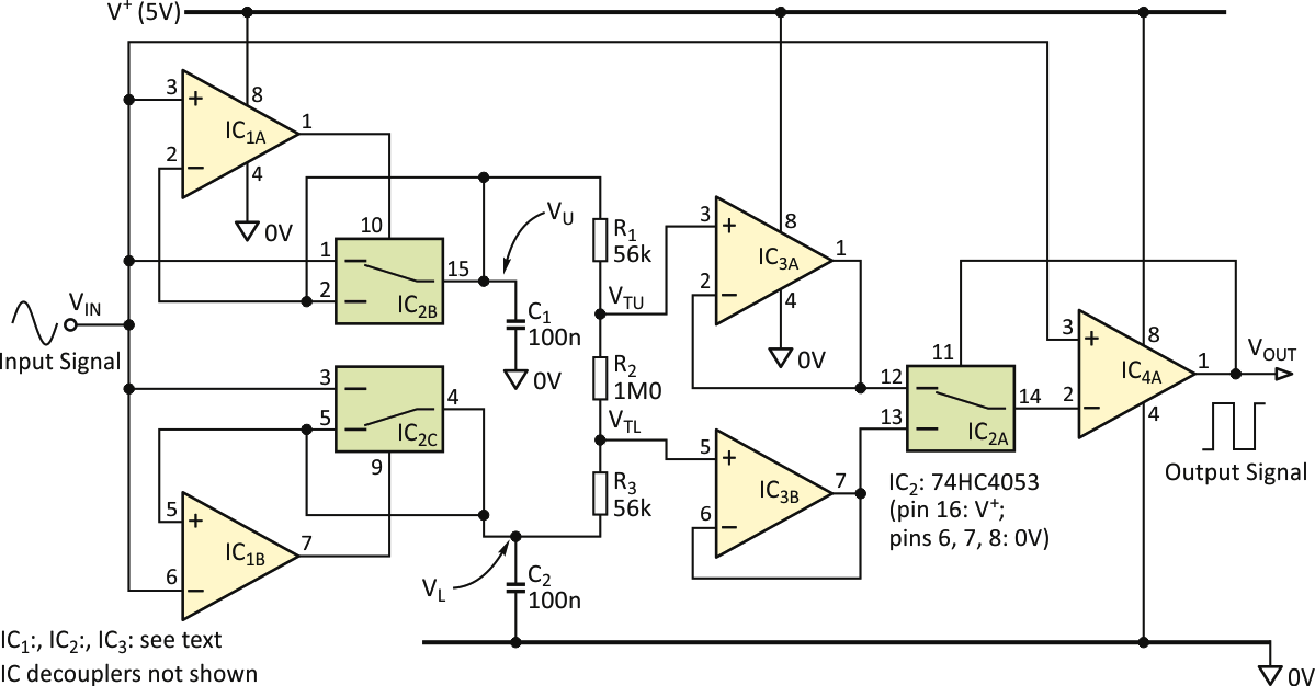
The Design Idea shown in Figure 1 solves these problems by implementing a circuit which automatically adjusts the trigger thresholds to suit the amplitude of the input signal. Comparator IC1A together with analog switch IC2B and capacitor C1 form a positive peak detector. When the input signal rises above the voltage stored on C1 at the comparator's inverting input, the comparator output goes high causing IC2B to switch into the position shown in the schematic. The detector now samples the input signal and tops up the charge stored on C1. When the input signal drops below the voltage on C1, the switch changes state such that the voltage VU stored on C1 is a DC level corresponding to the upper peak value of the input signal.
 |
|
| Figure 1. | Self-adaptive Schmitt trigger. |
Comparator IC1B, analog switch IC2C and capacitor C2 form a negative peak detector. This operates in the same way as the positive peak detector described above, but instead sampling on the negative peaks of the signal, such that the voltage VL stored on C2 is a DC level corresponding to the lower trough value of the input signal.
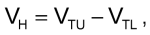
The resistor network formed by R1, R2, and R3 provides a discharge path for the charge stored on the sampling capacitors and also sets the upper and lower threshold voltages, VTU and VTL respectively, for the final comparator IC4A. The resistor values are chosen such that VTU is just slightly less than VU, and VTL is just slightly greater than VL. If we set R1 equal to R3, the voltage difference in percentage terms is given by:

With the values shown in the figure, VTU is 5% less than VU, and VTL is 5% greater than VL. In this way, the thresholds are constantly adjusted to track the input signal amplitude and DC level. For example, a 1 V peak-peak signal riding on a DC level of 2 V (i.e., VU = 2.5 V and VL = 1.5 V) would produce thresholds of VTU = 2.45 V and VTL = 1.55 V. It can be seen that the hysteresis voltage VH given by
(in this example 0.9 V) is always just slightly less than the peak-peak amplitude of the input signal.
The threshold voltages are buffered by before being fed to analog switch IC2A. To understand how the final part of the circuit works, assume that IC2A is in the state shown in the figure such that threshold voltage VTU is fed to the comparator's inverting input, and that the input signal at the comparator's non-inverting input is rising up from its negative peak. The digital output signal, VOUT, is currently at its low level. At the moment when the input signal just crosses VTU, the comparator output immediately goes high causing IC2A to change state and feed VTL to the comparator's inverting input. This positive feedback – typical of Schmitt trigger behaviour – ensures rapid, clean switching of the digital output signal. Buffers IC3A and IC3B are necessary (particularly at high frequencies) to prevent stray capacitance around IC4A's inverting input from introducing aberrations into VTU and VTL when IC2A changes state.
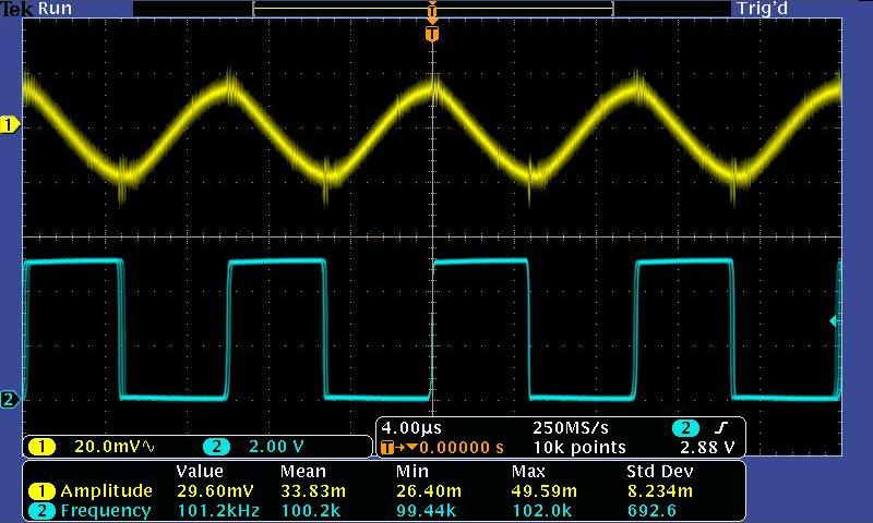
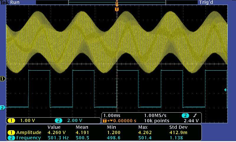
The oscillograms in Figures 2 and 3 show the performance of a test circuit built using comparators IC1 and IC4 = TLC3702 and op amp IC3 = TLC2272. These fairly extreme examples illustrate the circuit's ability to handle widely differing input signals.
In Figure 2, the source signal was a 500 Hz sinewave at 1.56 V P-P modulated by a 100 kHz sinewave at 2.88 V P-P, resulting in a composite signal of around 4.4 V P-P riding on a DC level of 2.5 V. Despite the “noise” amplitude being almost double the source amplitude, the circuit output switches cleanly at the source frequency and is completely unaffected by the HF modulation.
Figure 3 shows the circuit's response to very small input signals. Here, the source signal is a 100 kHz sinewave at around 30 mV P-P riding on a DC level of 400 mV. The presence of switching spikes in the input signal (due to less-than-perfect breadboard layout) results in some jitter in the output signal. Note that the input signal in Figure 2 is over a hundred times larger than that in Figure 3. In fact, provided the input signal remains within the common mode range of the comparators and buffers (in this case, around 0 to 4 V), the circuit can handle different signal amplitudes that vary by as much as two orders of magnitude. AC coupling is only required if the signal's DC level is outside the input common mode range.
 |
 |
||
| Figure 2. | 500 Hz signal with modulation "noise". | Figure 3. | Low amplitude input. |
You should choose C1 and C2 to suit the anticipated frequency range. Values of around 100 nF are suitable for frequencies above 300 Hz or so. Below this level, the sampling capacitance should be increased to prevent excessive decay ripple appearing on VU and VL. The TLC3702 comparators work well up to around 100 kHz, but beyond this level you may need faster devices.
Be aware that when the positive peak detector samples the input signal, capacitor C1 takes a gulp of charge from the input; the associated current that flows from the input is limited only by the on-resistance of IC2B. The same process occurs on the negative peaks with C2 and IC2C. If the input source impedance is significant, these current pulses can produce spikes in the input signal which can lead to erratic triggering. Therefore, it may be necessary to buffer the input signal to avoid these problems.
The circuit is not a panacea for all triggering applications, but it should prove useful for cases where the fixed thresholds of the conventional Schmitt trigger are not suitable. If it were not for my lack of temerity, and the confusion it might cause, I would suggest calling it the Smith Trigger.
