Joel Shetton
EDN
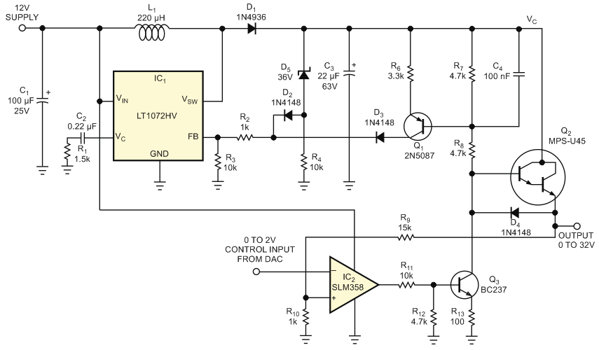
The circuit in Figure 1 delivers programming voltages to an EEPROM under the control of an external DAC (not shown). You can replace the DAC with a potentiometer to create a general-purpose power supply operating from 12 V and able to deliver a variable output voltage of 0 to 32 V. As Figure 1 shows, a Linear Technology LT1072HV variable-boost switching regulator, IC1, drives a Class A amplifier comprising operational amplifier IC2, voltage-boost-stage Q3, and emitter-follower Darlington transistor Q2. Resistors R9 and R10 set the amplifier's noninverting loop gain to a value of 1+(R9/R10).
 |
|
| Figure 1. | Able to deliver a wide range of output voltages, this regulator circuit automatically selects a linear or a switched mode as required. |
For output voltages below 8 V, switching regulator IC1 remains in shutdown mode, and the output stage draws current through L1 and D1. Q1's collector voltage, VC, measures approximately 11.4 V – that is, 12 V minus D1's forward-voltage drop. Transistor Q1 monitors the voltage drop across R7, which measures a fraction of Q2's collector-base voltage, VCB. As long as VCB exceeds 1 V, Q1's collector current remains high enough to drive IC1's feedback input higher than 1.25 V, which in turn keeps IC1 shut down.
As the output voltage increases, the voltage differential across R7 decreases, and, when it drops below 0.9 V, Q1's collector current decreases, lowering the feedback voltage applied to IC1 and switching it on. The boost regulator's output voltage increases, and the Q1- IC1 feedback loop regulates the collector-emitter voltage differential across Q2 to a constant 3 V for all outputs exceeding 8 V. If IC2's output goes to ground, cutting off Q3 and forcing Q2 into saturation, the feedback loop around Q1 opens and allows the circuit's output voltage to increase. Diode D5 and associated components form an overvoltage-protection clamp that limits IC1's output to 37 V.
Resistive divider R9 and R10 and IC2 determine the output voltage's range. Apart from selecting the VCE ratings of Q1 and Q3 to withstand the highest desired output voltage, values of other components are not critical. If you substitute appropriate components for D5, Q1, and Q3, the circuit can deliver output voltages as high as IC1's maximum output-switch rating – 75 V for the LT1072HV variant – minus 3 V.
