Steven Galecki
Electronic Design
This circuit automatically attenuates a high voltage by known factors so that it matches the ADC input range for best converter resolution.
It's a common challenge to measure voltages that exceed the operating voltage of the ADC used as part of the measurement circuit. One commonly employed method is to use a resistor string as a voltage divider, setting the resistor ratio such that the highest voltage of interest is scaled below the ADC’s reference voltage. It provides a fixed ratio, but small input voltages can’t take advantage of the dynamic range of the ADC. Also, unanticipated oversized signals may damage the input of the ADC circuit, as well as distort the signal due to changes in the circuit’s impedance.
The alternative circuit approach discussed here scales the input voltage using multiple voltage dividers to maximize measurement accuracy. It takes advantage of the fact that the signal source for this circuit is a current sink that feeds a defined range of load impedances (resistances).
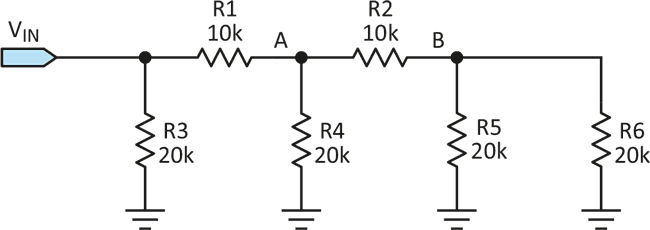
The voltage divider used is based on an R-2R circuit (Fig. 1). Each leg of the divider (or top of a 20-kΩ resistor) will have one-half the voltage of the previous leg. The voltage at A is half the voltage at VIN, and the voltage at B is half the voltage at A. Each leg also carries one-half the current of the previous leg. The current through R5 is half the current through R4, which is half the current through R3, and the current through R3 is half the total current coming into the R-2R circuit. In addition, the input impedance of the circuit will be 10 kΩ.
 |
||
| Figure 1. | The design's principle is based on an R-2R circuit used to create multiple attenuation points. |
|
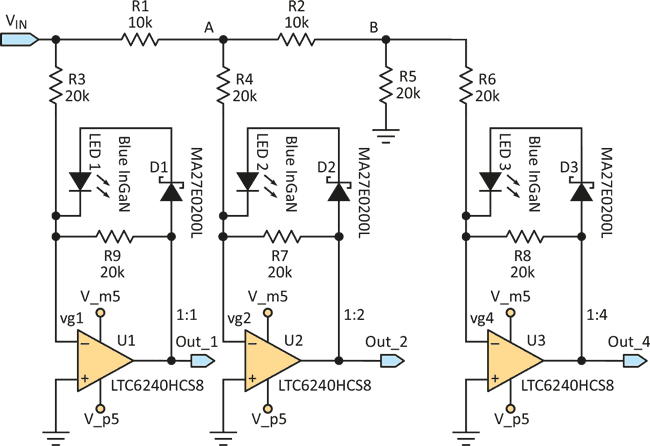
The voltage at the different nodes of the resistor-divider network (VIN, A, B) may be higher than the reference voltage of the data converter. Rather than measuring the voltages on the nodes, this circuit measures the current through each leg. Three op amps are used to create virtual grounds for the resistor network; these op amps mirror the current flowing through resistors R3, R4, and R6 (Fig. 2).
 |
||
| Figure 2. | Op amps are used to create the virtual grounds needed to make the R-2R circuit work in the configuration. A pair of diodes is used with each op amp's feedback path to limit the voltage drop across the feedback resistor. |
|
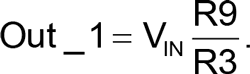
U1 changes the voltage on Out_1 (and the current through resistor R3 and feedback resistor (R9) so that U1’s negative input is at the same voltage as U1’s positive input. The output voltage of U1 is
To limit the voltage drop across the feedback resistor to approximately 2 V, two diodes in series (a blue LED and a Schottky diode) are placed in parallel with R9.
Leakage current reduces the accuracy of the voltage across the feedback resistor, but the blue LED has very low leakage current. The low capacitance of the Schottky diode (≈2 pF at 0 V) reduces the capacitive loading of the LED on the feedback loop. Similar circuits are used on the other legs of the R-2R circuit.
 |
||
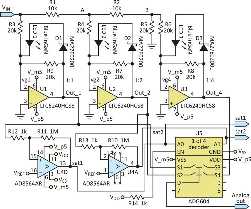
| Figure 3. | Shown is the complete design of the R-2R circuit with op-amps feeding comparators and an analog multiplexer. |
|
The output voltage from the op amp then feeds two circuits (Fig. 3). The first circuit is a comparator with a threshold at VREF. The comparator changes state when the op-amp output voltage exceeds VREF, and its output provides information to the controller regarding the gain of the analog signal. The output of the op amps also goes to an input of U5, an analog multiplexer, whose output is determined by the comparator with the largest input signal that hasn’t exceeded VREF (see Table 1).
| Table 1. | Output of analog multiplexer driven by comparators. | |||||||||||||||
|
||||||||||||||||
If U1’s signal is the appropriate signal to feed into an ADC, then the voltage is not scaled (1:1) and the MSB of the ADC represents ½ VREF. If U1 saturates, then the signal from U2 is used. The signal to the ADC is reduced by 2:1 and the MSB of the ADC represents VREF, which is accomplished by performing a left shift on the ADC data. If U2 also saturates, then the signal from the U3 is used. The signal to the ADC reduces by 4:1 and the MSB of the ADC represents 2 × VREF, in which case the ADC data shifts two bits to the left.
This circuit allows the signal to be measured with the full accuracy of the ADC within each range. A 1.0-V signal could be measured with 10-bit accuracy using a VREF of 1.25 V (approximately 1.25 mV/bit), while a 4.0-V signal could also be measured with 10-bit accuracy (approximately 5 mV/bit) using the same ADC converter. The circuit also self-selects the appropriate gain of the signal while not overdriving the measurement circuitry during large signals.
