You use a JFET's self-biasing characteristics to build a dc/dc converter that operates from power sources such as solar cells, thermopiles, and single-stage fuel cells, all of which deliver less than 600 mV and sometimes as little as 300 mV. Figure 1 shows the drain-to-source characteristics of an N-channel JFET under zero-bias conditions, which you can produce by connecting its gate and source together. Applying 100 mV causes a current of 10 mA to flow through the device, increasing to 30 mA at 300 mV. Exploiting the JFET's ability to conduct significant current at zero bias makes it possible to design a self-starting, low-input-voltage converter.
 |
||
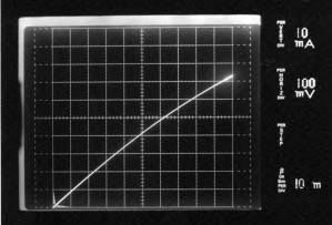
| Figure 1. | At 100 mV between drain and source (horizontal axis), the drain current reaches 10 mA (vertical axis) and increases to 30 mA at 300 mV. |
|
The circuit can supply 5 V at currents as large as 2 mA – enough to serve many micropowered applications or to provide auxiliary bias for a higher power switched-mode voltage regulator. At 300-mV input, the circuit starts up at load currents of 300 µA. A load current of 2 mA requires an input of 475 mV.
 |
||
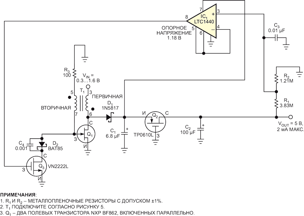
| Figure 2. | A pair of parallel-connected JFETs allows this dc/dc converter to operate from power sources that supply as little as 300 mV. |
|
In Figure 2, Q1, a parallel-connected pair of NXP's BF862 JFETs, and Coiltronics' Versa-Pac transformer, T1, form an oscillator in which T1's secondary winding provides feedback to Q1's gate. When you first apply power, Q1's gate rests at 0 V, and drain current flows through T1's primary winding. T1's phase-inverted secondary winding responds by delivering a negative voltage to Q1's gate, which turns off Q1 and interrupts current flow through T1's primary winding. In turn, T1's secondary voltage collapses, and sustained oscillations begin. Although the BF862's published specifications do not cover the device's internal geometry, the device has a low on-resistance and maintains a low gate-turn-on threshold voltage. Using a pair of parallel-connected JFETs for Q1 ensures the low saturation voltage for operation at low power-supply voltages.
 |
||
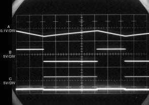
| Figure 3. | The dc output (Trace A), comparator IC1’s output (Trace B), and the voltage at Q1’s drain (Trace C) have a horizontal-deflection factor of 5 msec. |
|
Rectifying and filtering the positive-going flyback-voltage impulses on Q1's drain produce a dc voltage across capacitor C1. To assist the circuit's start-up, a P-channel MOSFET, Q2, which requires a gate-to-source voltage of approximately 2 V for conduction, initially isolates the output load from the rectifier. When Q2 conducts, the output voltage increases toward 5 V. Comparator IC1, a Linear Technology LTC1440, draws power from Q2's source and imposes output-voltage regulation by comparing its internal voltage reference with a sample of the output voltage. The output from IC1 varies Q1's on-time through Q3 to close the control loop and maintain output-voltage regulation. Figure 3 shows the ripple voltage present at the power supply's output. When the output voltage decays, comparator IC1 switches (Trace B, middle) and allows Q1 to oscillate. The resulting flyback events at Q1's drain (Trace C, bottom) restore the output voltage.
 |
||
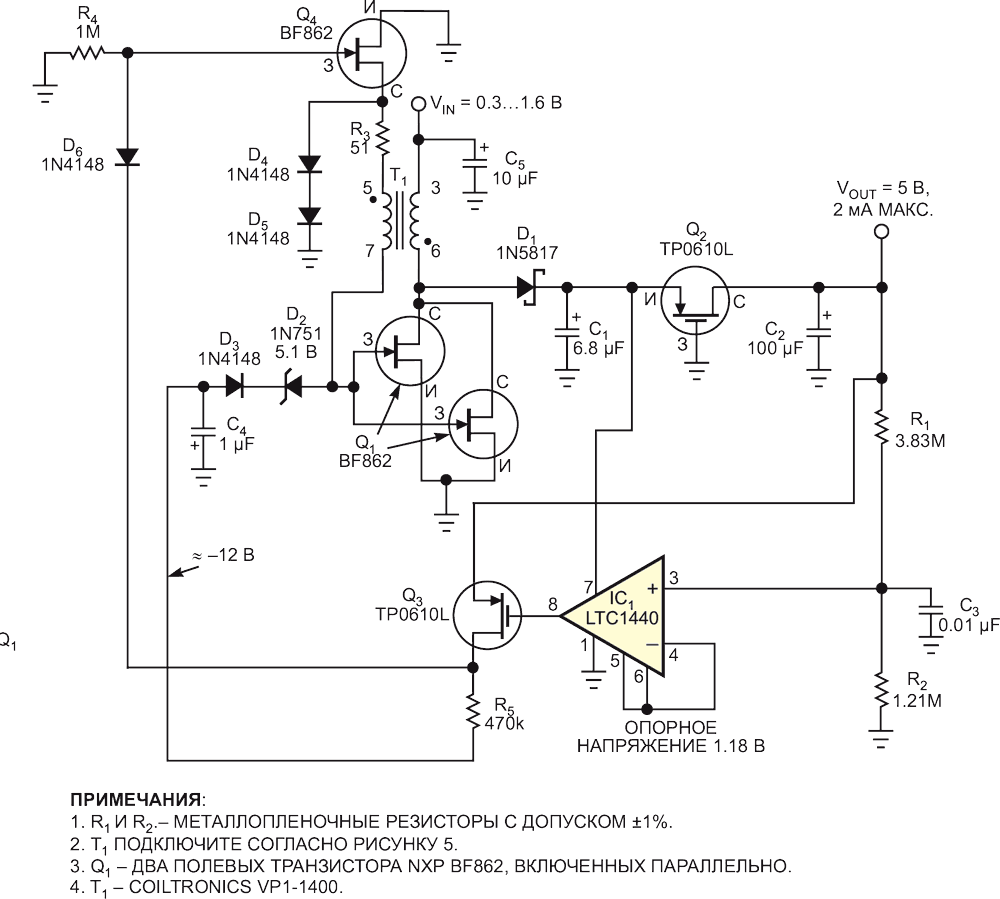
| Figure 4. | Adding Q3, Q4, and the bootstrapped negative-bias generator comprising D2, D3, and C4 reduces the circuit’s quiescent current from 25 mA to 1 mA. |
|
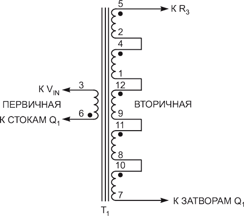
Using Q3 as a simple but effective shunt control for Q1's gate voltage results in a 25-mA quiescent-current drain from the power source. A modification reduces the quiescent drain to 1 mA (Figure 4). Inserting switch Q4 in series with T1's secondary winding more efficiently controls Q1's gate. Bootstrapping the voltage across T1's secondary winding produces negative-turn-off-bias voltage for Q4. Figure 5 illustrates how to connect T1's windings. When Q4 switches off, it interrupts the current flowing in T1's secondary winding and drives T1's Pin 5 positive. Without diodes D4 and D5, the peak voltage would approach 15 V and reverse-bias Q4, an undesirable condition. Under normal operating conditions, excursions of approximately 0.8 V appear at Pin 5, necessitating the use of two series-connected diodes to clamp the voltage at a safe level. Zener diode D2 holds off bias-supply loading to aid start-up during initial power application.
 |
||
| Figure 5. | Comprising six independent windings that offer more than 500 configurations, Coiltronics’ VP1-1400 serves as a combination feedback and flyback transformer in this application. Connect the windings as shown. |
|
