Arturo Rivera
EDN
This Design Idea avoids the RC charging waveshape of a standard relaxation oscillator, replacing it with a linear rise/fall triangle wave. Positive feedback is used to increase the charging rate over each half-cycle and straighten out the curve.
The oscillator consists of Schmitt trigger comparator U1 and non-inverting adder U2. Oscillation is accomplished by the same principle that drives the relaxation oscillator, toggling the comparator output when the capacitor voltage reaches the threshold of the hysteresis. This hysteresis voltage, VH, is defined by R1 & R2 in the comparator’s positive feedback loop.
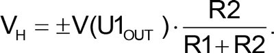
The hysteresis band sets the amplitude of the triangular waveform across C1.
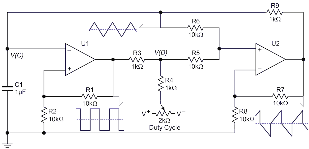
The comparator output is a rectangular wave whose amplitude is dependent on U1’s output stage. This signal is reduced by R3 & R4 before the adder; otherwise, the triangular shape will revert to the RC curve.
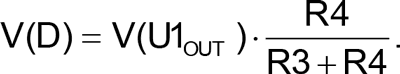
Since V(D) must be stable, R3 & R4 are several times lower than the surrounding resistors; R3+R4 is the comparator’s main load. Low values (here 1 kΩ) are suggested, commensurate with acceptable U1 output loading, though all values can be scaled up.
The U2 adder sums V(D) and the capacitor voltage V(C) with a gain of two, defined by R7 & R8. Its output charges C1 through R9. With V(D) at ±½V(U1OUT), the capacitor voltage will describe a linear-slope line, forming a triangular waveform.
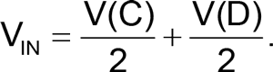
The adder input resistors R5 & R6 divide both voltages by two. The Barkhausen stability criterion requires unity gain to perform oscillation, so the adder gain must recover this loss:
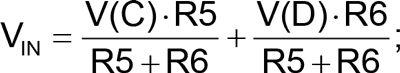
if R5 = R6 then:
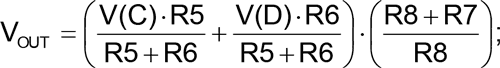
If R5 = R6 and R7 = R8 then

The addition process can be described as two time functions: one from T0 to T1, where V(C)T0 = –VH and V(C)T1 = +VH due to the positive value of V(D), and the other from T1 to T2, which reverses the process: V(C)T2 = –VH, due to the negative value of V(D). Each integral must equal zero because a DC offset is not expected.
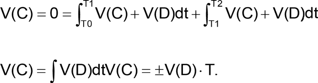
Solving the general form of the equation, where V(C) initial value is zero and V(D) toggles between positive and negative: The solution for V(C) is a linear function of V(D) and time. V(D) toggles between positive and negative when it reaches ±VH. If V(D) increases, the frequency will increase too.
| C1 | Frequency |
| 10µF | 10-50 Hz |
| 1µF | 100-500 Hz |
| 0.1µF | 1-5 kHz |
| 0.01µF | 10-50 kHz |
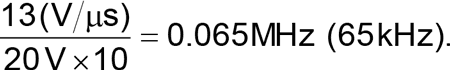
The op-amp’s slew rate limits the frequency of this application. The comparator output must maintain a square shape, so the minimum period can be defined using the total excursion and a factor of 10:
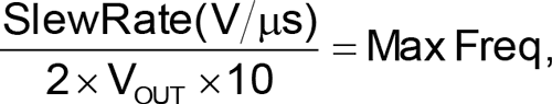
e.g.,
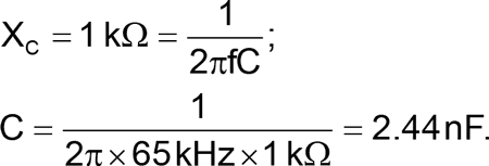
At this maximum frequency, the adder output current through R9 & C1 must be drivable by the op-amp. If necessary, calculate the RC impedance and C1 value – in this example, to meet 2 kΩ total: R9 = 1 kΩ, XC = 1 kΩ.
Output frequency is equal to:
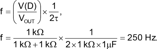
Duty-cycle adjustment is made by adding a DC component to V(D) through R4. The usable adjustment range is about 10%-90%.