Fabio Cacciotto, STMicroelectronics
EDN
Modern appliances offer a range of features that rely heavily on microcontrollers and auxiliary circuits. Although conventional iron-core transformers can provide ac line-isolated, low-voltage power for a microprocessor, coupling the processor’s control signals to line-side power switches requires yet another layer of electrical isolation, such as optocouplers or pulse transformers.
Designers can avoid the complexity and expense of adding isolation components by powering the microcontroller and its auxiliary circuits from the non-isolated ac line. An offline SMPS (switched-mode power supply) can easily produce a single low voltage, but obtaining multiple voltages can prove more challenging and require a relatively complicated design.
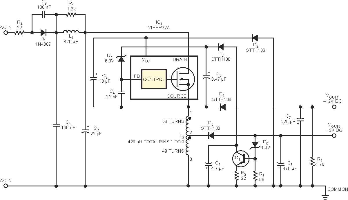
As an alternative, you can use a single-chip SMPS controller, such as STMicroelectronics’ Viper22A, IC1, to derive as much as 3.3 W of regulated dual-voltage power over an ac line-voltage range of 88 to 265 V ac (Figure 1). For the values in the figure, this circuit delivers –5 V ±5% at currents as high as 300 mA and –12 V ±10% at currents as high as 150 mA.
 |
||
| Figure 1. | This offline SMPS controller delivers dual output voltages. | |
The Viper22A’s internal circuitry includes a 60-kHz clock oscillator, a voltage reference, overtemperature protection, and a high-voltage power MOSFET that can provide several watts of power. Although the Viper22A occupies an eight-lead package, operating requires only four connections: operating power, VDD; feedback, FB; and the MOSFET’s source and drain. The remainder of the pins, redundant source and drain connections, help dissipate heat into the pc board.
Resistor R4 limits input surge current and doubles as a protective fuse. Diode D1 rectifies the ac line voltage, providing approximately 160 V dc to a filter comprising C1, R1, L1, and C2. In addition to smoothing dc ripple, the filter reduces electromagnetic interference to help achieve compliance with EU standard 55014 CISPR14. Snubber capacitor C9 across D1 helps further reduce conducted emissions.
Reservoir capacitor C3 acquires a positive charge via diode D3 during the MOSFET’s off-time and supplies VDD to IC1 during the MOSFET’s on-time. Reverse voltage across D3 can reach the sum of the peak rectified line voltage plus the magnitude of the maximum regulated dc output voltage, so use a fast-recovery diode rated for 600 V peak-inverse voltage for D3.
The voltage at VOUT2 provides feedback to close the regulation loop. The sum of general-purpose PNP transistor Q1’s base-emitter voltage plus D6’s reverse voltage sets VOUT2 at –5 V. Zener diode D7 shifts the voltage at IC1’s feedback input terminal into its linear range (0 to 1 V). To avoid high-frequency instability in the compensation loop, keep connections to ceramic capacitor C4 as short as possible. Inductor L2 comprises a TDK SRW0913 ferrite drum core with two windings whose turns ratio sets the output voltage at VOUT1. To maintain regulation when VOUT1 is unloaded and VOUT2 is fully loaded, add bleeder resistor R5 from VOUT1 to common ground.
