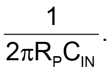
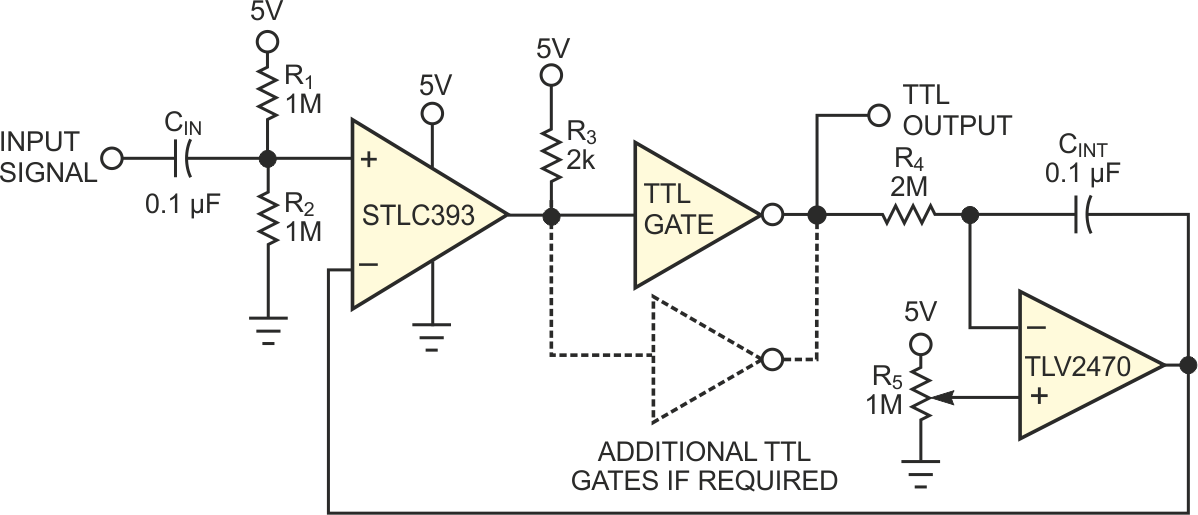
Converting periodic waveforms to square waves is an integral part of extracting a clock signal from data, creating waveform generators, and making timing-pulse generators. Any square-wave-conversion circuit is more valuable when the square wave's duty cycle is variable and controllable. Figure 1 shows a circuit that has these attributes and can drive several TTL-compatible loads. CIN couples the input signal onto a dc level set by R1 and R2 (the level is VCC/2 when R1 = R2). Thus, the periodic signal at the noninverting comparator input rises above and falls below VCC/2. The parallel value of R1 and R2 (RP) and CIN form a highpass filter with a -3-dB frequency of
Increasing RP or CIN lowers the cutoff frequency for low-frequency applications. If high-frequency noise riding on the signal causes problems, add a capacitor in parallel with R2; this addition eliminates the high-frequency noise by creating a low-frequency filter. If the input signal is a square wave, the added capacitor integrates the square wave, thus increasing its rise and fall times. The longer rise and fall times give the circuit more control range.
 |
||
| Figure 1. | You can obtain a square wave with 2 to 98% duty cycle with this simple circuit. | |
When the input signals are symmetrical, setting the dc level at VCC/2 produces the maximum pulse-width control and duty-cycle range. Asymmetrical input signals require a different dc level, because the time durations of the positive and negative portions (with respect to VCC/2) of the coupled signal are not equal. RP's value must be low to prevent input-bias current from developing an appreciable offset voltage. The comparator in this design is a CMOS TLC393 version of the industry-standard LM393. The comparator weighs the dc-referenced input signal against a reference voltage from the integrator output. The comparator's output waveform is a square wave. The comparator drives a gate (or several gates if you need more output drive) through R3. R3 must have a low value to quickly charge the gate input during the low-to-high transition. The current the comparator can sink limits R3's lower value.
The TLV2470 integrator integrates and inverts the output square wave and feeds it back as the reference voltage for the input comparator. If the voltage on the positive-integrator input is VCC/2, the output square wave must be symmetrical for its average value to be VCC/2. Adjusting R5 to its center point yields a 50%-duty-cycle square wave. Adjusting R5 close to ground yields a square wave that is low for most of the period, and adjusting R5 close to VCC yields a square wave that is high for most of the period. The integrator pole is at
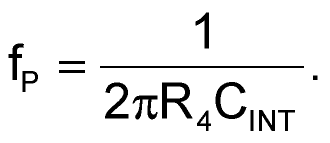
With the values shown in Figure 1, the 0-dB crossover frequency is 0.8 Hz. The gain of the integrator circuit is unity at 0.8 Hz, and the gain rolls off at 20 dB per decade, so the comparator's small-signal gain is not high enough to cause oscillation. The selection of the integrator pole is a trade-off between stability and control-response time. The circuit in Figure 1 does not oscillate or multiple-switch under any conditions. It produces a square wave that's adjustable from 2 to 98% duty cycle, and it responds to 20-mV input signals.
