Whenever I find myself harboring a constantly nagging thought, I know I will eventually have to get busy and find a way to put it to rest.
When I read EDN’s Design Ideas, I look for the range of frequencies over which the circuit will operate, if this is an appropriate spec for the circuit. Mentally, I give the circuit a low score if the operating frequency range is, in my opinion, limited.
My nagging thought was “can the operating frequency range for the Frequency doubler with 50 percent duty cycle (Reference 1) be significantly extended above 2.82 MHz?” If “yes”, then can it be done for a “reasonable” cost? (Reasonable cost, of course, depends on the application, among other things, some of which may be somewhat subjective.)
So, I started thinking and researching possible ways to extend the frequency range of the recently published square wave frequency doubler circuit.
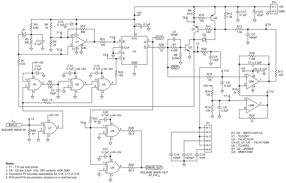
To extend the operating frequency range, I needed to begin with a really fast one-shot circuit. Being unable to purchase a suitable device, I designed one similar to the ubiquitous 555 timer, but with much faster components. Fast XOR gates, a fast comparator, a fast flip-flop, and a fast discharge transistor are the main components of the one-shot. This one-shot circuit will operate at frequencies up to 50 MHz (and probably even higher).
The comparator I used, the TLV3501 from Texas Instruments, operates rail-to-rail (input and output), and has a typical prop delay of 4.5 ns (6.4 ns max) when driving 17 pF.
It is the costliest component used in my circuit ($1.62 in 1k quantity), but it is fast, reasonably priced, and readily available. The other components are inexpensive, fast, and widely used in the electronics industry. (The MMBT2369 is the surface mount version of the 2N2369, which dates back to the early 1960s, but it is pretty fast and it is cheap.)
The 74LVC1Gxx parts have prop delay times in the order of 1 ns when driving a few picofarads of capacitance, and they can be operated with a supply voltage of 5 V (which was my preference). I used the TLV9052 dual op amp, which has infinite input impedance (well, almost) and operates rail-to-rail, input and output. The 74LVC1G86 XOR gate is handy because it can function as an inverter or as a buffer, and I used several of them.
A simple description of the operation of the circuit: An ultra-fast one-shot is forced by negative feedback to produce a 50% duty cycle square wave output. I added a 50-ohm termination and a buffer/squarer at the input and a 50-ohm driver at the output for convenience in testing.
The nitty-gritty description (Figure 1): A 50% duty cycle square wave is the input to the XOR gate, U3 (via U7), causing a 2 ns pulse output from U5 to be applied to the /S input of the flip-flop, U2. The /Q output of the flip-flop goes low and turns off the discharge transistor, Q3, which allows the timing capacitor, C4, to begin charging. The output from Q3 is a voltage ramp which is applied through R1 to the inverting input of comparator, U1. The output of the comparator goes low when the voltage ramp reaches the reference voltage set by R4 and R5. This resets the flip-flop, causing the discharge transistor to turn on and discharge the timing capacitor, C4, and the cycle repeats.
 |
|
| Figure 1. | Circuit for an ultra-fast one-shot is forced by negative feedback to produce a 50% duty cycle square wave output. |
The charging current to C4 is supplied by Q1 and the associated components. The charging current is controlled by negative feedback from op amp U6A, which forces the one-shot to produce a square wave of 50% duty cycle, which, when low-pass filtered, produces a DC voltage of exactly 2.5 V (if the supply voltage is exactly 5 V). The tolerances of R18 and R19 will determine how exact this voltage is.
The reference voltage provided by U6B and its associated components is set to 2.5 V by precision (or matched) resistors R18 and R19. This reference will track the +5 V supply, so that the 50% duty cycle square wave output of the circuit remains at 50% if the supply voltage changes. (The lightly loaded output of the flip-flip also tracks changes in the supply voltage.)
Simulation, implementation, testing, and results
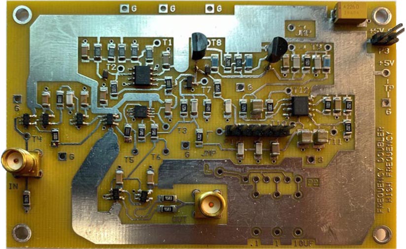
I used LTspice to design and simulate the circuit. Then I used Express PCB’s free tools to design and lay out a two-sided circuit board with a ground plane on the bottom side. I used AppCad, which is freely available on the web, to simulate the signal’s overshoot/undershoot on critical traces. I inserted resistors in series with some of the longer traces for fast signals to reduce overshoot/undershoot. I used surface mount devices for all of the components except Q1, Q2, the input and output SMA connectors, and connecter P1 and P3. (P2 was not used.) The points marked T1 through T12 are test points (plated-thru holes on the PCB). The loaded circuit board is shown in Figure 2.
 |
|
| Figure 2. | The loaded two-sided circuit board with a ground plane on the bottom side, the points marked T1 through T12 are test points. |
The 10 pF capacitor for C4 was left in the circuit when I tested with other values of C4. The other values were soldered on the PCB, but were connected to a 0.100-inch center connector mounted on the PCB, so I could select them individually with a slide-on shorting tab. That is why all the other values of C4 have an additional 10 pF for the frequency range tests.
The circuit performance was pretty well predicted by the LTspice and AppCad simulations. Table 1 shows the range of performance vs several values of C4.
| Table 1. | The range of performance with different values of C4 |
||||||||||
|
|||||||||||
This circuit extends the operating frequency range for the frequency doubler to 36 MHz, which is more than 10 times the upper frequency limit of the original circuit.
Reference
- McLucas, Jim. “Frequency doubler with 50 percent duty cycle.“