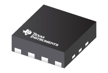
Datasheet Texas Instruments TPS61021ADSGT
| Manufacturer | Texas Instruments |
| Series | TPS61021A |
| Part Number | TPS61021ADSGT |

3-A Boost Converter with 0.5-V Ultra Low Input Voltage 8-WSON -40 to 125
Datasheets
TPS61021A 3-A Boost Converter with 0.5-V Ultra Low Input Voltage datasheet
PDF, 5.5 Mb, File published: Jun 1, 2016
Extract from the document
Status
| Lifecycle Status | Active (Recommended for new designs) |
| Manufacture's Sample Availability | No |
Packaging
| Pin | 8 |
| Package Type | DSG |
| Industry STD Term | WSON |
| JEDEC Code | S-PDSO-N |
| Package QTY | 250 |
| Carrier | SMALL T&R |
| Device Marking | 11G |
| Width (mm) | 2 |
| Length (mm) | 2 |
| Thickness (mm) | .75 |
| Pitch (mm) | .5 |
| Max Height (mm) | .8 |
| Mechanical Data | Download |
Parametrics
| Duty Cycle(Max) | 90 % |
| Iq(Typ) | 0.017 mA |
| Operating Temperature Range | -40 to 125 C |
| Package Group | WSON |
| Rating | Catalog |
| Regulated Outputs | 1 |
| Special Features | Enable,Light Load Efficiency,Load Disconnect,Synchronous Rectification |
| Switch Current Limit(Min) | 3 A |
| Switch Current Limit(Typ) | 4.3 A |
| Type | Converter |
| Vin(Max) | 4.4 V |
| Vin(Min) | 0.5 V |
| Vout(Max) | 4 V |
| Vout(Min) | 1.8 V |
Eco Plan
| RoHS | Compliant |
Design Kits & Evaluation Modules
- Evaluation Modules & Boards: TPS61021EVM-723
Boost Converter Evaluation Module for TPS61021A
Lifecycle Status: Active (Recommended for new designs)
Application Notes
- Single LED Driver in AA Battery-Powered SystemsPDF, 1.6 Mb, File published: Aug 25, 2017
- Feedforward Capacitor Makes Boost Converter Fast and StablePDF, 1.0 Mb, File published: Nov 2, 2016
- Minimizing Ringing at the Switch Node of a Boost ConverterPDF, 201 Kb, File published: Sep 15, 2006
The application report explains how to use proper board layout and/or a snubber to reduce high-frequency ringing at the switch node of a boost converter. - Design considerations for a resistive feedback divider in a DC/DC converterPDF, 393 Kb, File published: Apr 26, 2012
- Basic Calculation of a Boost Converter's Power Stage (Rev. C)PDF, 186 Kb, Revision: C, File published: Jan 8, 2014
This application note gives the equations to calculate the power stage of a boost converter built with an IC with integrated switch and operating in continuous conduction mode. It is not intended to give details on the functionality of a boost converter (see Reference 1) or how to compensate a converter. See the references at the end of this document if more detail is needed. - Optimizing Transient Response of Internally Compensated DC-DC Converters (Rev. A)PDF, 1.1 Mb, Revision: A, File published: May 11, 2015
- Choosing an Appropriate Pull-up/Pull-down Resistor for Open Drain OutputsPDF, 130 Kb, File published: Sep 19, 2011
- QFN and SON PCB Attachment (Rev. B)PDF, 821 Kb, Revision: B, File published: Aug 24, 2018
- IQ: What it is what it isn’t and how to use itPDF, 198 Kb, File published: Jun 17, 2011
- Performing Accurate PFM Mode Efficiency Measurements (Rev. A)PDF, 418 Kb, Revision: A, File published: Dec 11, 2018
When performing measurements on DC-DC converters using pulse frequency modulation(PFM)or any power save mode proper care must be taken to ensure that the measurements are accurate. An accurate PFM mode efficiency measurement is critical for systems which require high efficiency at low loads such as in smart home systems tablets wearables and metering.
Model Line
Series: TPS61021A (2)
- TPS61021ADSGR TPS61021ADSGT
Manufacturer's Classification
- Semiconductors > Power Management > Non-isolated DC/DC Switching Regulator > Step-Up (Boost) > Boost Converter (Integrated Switch)