Datasheet Texas Instruments CD74AC20
| Manufacturer | Texas Instruments |
| Series | CD74AC20 |
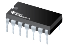
Dual 4-Input NAND Gates
Datasheets
CD74AC20 datasheet
PDF, 594 Kb, Revision: B, File published: Nov 15, 2002
Extract from the document
Prices
Status
| CD74AC20E | CD74AC20M | CD74AC20M96 | CD74AC20M96E4 | CD74AC20M96G4 | CD74AC20MG4 | |
|---|---|---|---|---|---|---|
| Lifecycle Status | Active (Recommended for new designs) | Active (Recommended for new designs) | Active (Recommended for new designs) | Active (Recommended for new designs) | Active (Recommended for new designs) | Active (Recommended for new designs) |
| Manufacture's Sample Availability | No | No | No | No | No | No |
Packaging
| CD74AC20E | CD74AC20M | CD74AC20M96 | CD74AC20M96E4 | CD74AC20M96G4 | CD74AC20MG4 | |
|---|---|---|---|---|---|---|
| N | 1 | 2 | 3 | 4 | 5 | 6 |
| Pin | 14 | 14 | 14 | 14 | 14 | 14 |
| Package Type | N | D | D | D | D | D |
| Industry STD Term | PDIP | SOIC | SOIC | SOIC | SOIC | SOIC |
| JEDEC Code | R-PDIP-T | R-PDSO-G | R-PDSO-G | R-PDSO-G | R-PDSO-G | R-PDSO-G |
| Package QTY | 25 | 50 | 2500 | 2500 | 2500 | 50 |
| Carrier | TUBE | TUBE | LARGE T&R | LARGE T&R | LARGE T&R | TUBE |
| Device Marking | CD74AC20E | AC20M | AC20M | AC20M | AC20M | AC20M |
| Width (mm) | 6.35 | 3.91 | 3.91 | 3.91 | 3.91 | 3.91 |
| Length (mm) | 19.3 | 8.65 | 8.65 | 8.65 | 8.65 | 8.65 |
| Thickness (mm) | 3.9 | 1.58 | 1.58 | 1.58 | 1.58 | 1.58 |
| Pitch (mm) | 2.54 | 1.27 | 1.27 | 1.27 | 1.27 | 1.27 |
| Max Height (mm) | 5.08 | 1.75 | 1.75 | 1.75 | 1.75 | 1.75 |
| Mechanical Data | Download | Download | Download | Download | Download | Download |
Parametrics
| Parameters / Models | CD74AC20E | CD74AC20M | CD74AC20M96 | CD74AC20M96E4 | CD74AC20M96G4 | CD74AC20MG4 |
|---|---|---|---|---|---|---|
| Bits | 2 | 2 | 2 | 2 | 2 | 2 |
| F @ Nom Voltage(Max), Mhz | 100 | 100 | 100 | 100 | 100 | 100 |
| ICC @ Nom Voltage(Max), mA | 0.04 | 0.04 | 0.04 | 0.04 | 0.04 | 0.04 |
| Operating Temperature Range, C | -55 to 125 | -55 to 125 | -55 to 125 | -55 to 125 | -55 to 125 | -55 to 125 |
| Output Drive (IOL/IOH)(Max), mA | 24/-24 | 24/-24 | 24/-24 | 24/-24 | 24/-24 | 24/-24 |
| Package Group | PDIP | SOIC | SOIC | SOIC | SOIC | SOIC |
| Package Size: mm2:W x L, PKG | See datasheet (PDIP) | 14SOIC: 52 mm2: 6 x 8.65(SOIC) | 14SOIC: 52 mm2: 6 x 8.65(SOIC) | 14SOIC: 52 mm2: 6 x 8.65(SOIC) | 14SOIC: 52 mm2: 6 x 8.65(SOIC) | 14SOIC: 52 mm2: 6 x 8.65(SOIC) |
| Rating | Catalog | Catalog | Catalog | Catalog | Catalog | Catalog |
| Schmitt Trigger | No | No | No | No | No | No |
| Technology Family | AC | AC | AC | AC | AC | AC |
| VCC(Max), V | 5.5 | 5.5 | 5.5 | 5.5 | 5.5 | 5.5 |
| VCC(Min), V | 1.5 | 1.5 | 1.5 | 1.5 | 1.5 | 1.5 |
| Voltage(Nom), V | 1.5,3.3,5 | 1.5,3.3,5 | 1.5,3.3,5 | 1.5,3.3,5 | 1.5,3.3,5 | 1.5,3.3,5 |
| tpd @ Nom Voltage(Max), ns | 139,15.5,11.1 | 139,15.5,11.1 | 139,15.5,11.1 | 139,15.5,11.1 | 139,15.5,11.1 | 139,15.5,11.1 |
Eco Plan
| CD74AC20E | CD74AC20M | CD74AC20M96 | CD74AC20M96E4 | CD74AC20M96G4 | CD74AC20MG4 | |
|---|---|---|---|---|---|---|
| RoHS | Compliant | Compliant | Compliant | Compliant | Compliant | Compliant |
| Pb Free | Yes |
Application Notes
- Using High Speed CMOS and Advanced CMOS in Systems With Multiple VccPDF, 43 Kb, File published: Apr 1, 1996
Though low power consumption is a feature of CMOS devices sometimes this feature does not meet a designer?s system power supply constraints. Therefore a partial system power down or multiple Vcc supplies are used to meet the needs of the system. This document shows electrostatic discharge protection circuits. It also provides circuit and bus driver examples of partial system power down and curren
Model Line
Series: CD74AC20 (6)
Manufacturer's Classification
- Semiconductors> Logic> Gate> NAND Gate
