Datasheet Texas Instruments SN74ALVC08
| Manufacturer | Texas Instruments |
| Series | SN74ALVC08 |
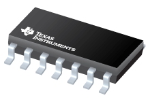
Quadruple 2-Input Positive-AND Gate
Datasheets
SN74ALVC08 datasheet
PDF, 778 Kb, Revision: I, File published: Aug 31, 2004
Extract from the document
Prices
Status
| SN74ALVC08D | SN74ALVC08DG4 | SN74ALVC08DGVR | SN74ALVC08DR | SN74ALVC08DRE4 | SN74ALVC08DRG4 | SN74ALVC08NSR | SN74ALVC08PWR | SN74ALVC08PWRE4 | SN74ALVC08PWRG4 | SN74ALVC08RGYR | SN74ALVC08RGYRG4 | |
|---|---|---|---|---|---|---|---|---|---|---|---|---|
| Lifecycle Status | Active (Recommended for new designs) | Active (Recommended for new designs) | Active (Recommended for new designs) | Active (Recommended for new designs) | Active (Recommended for new designs) | Active (Recommended for new designs) | Active (Recommended for new designs) | Active (Recommended for new designs) | Active (Recommended for new designs) | Active (Recommended for new designs) | Active (Recommended for new designs) | Active (Recommended for new designs) |
| Manufacture's Sample Availability | No | No | No | Yes | No | Yes | No | No | No | No | No | No |
Packaging
| SN74ALVC08D | SN74ALVC08DG4 | SN74ALVC08DGVR | SN74ALVC08DR | SN74ALVC08DRE4 | SN74ALVC08DRG4 | SN74ALVC08NSR | SN74ALVC08PWR | SN74ALVC08PWRE4 | SN74ALVC08PWRG4 | SN74ALVC08RGYR | SN74ALVC08RGYRG4 | |
|---|---|---|---|---|---|---|---|---|---|---|---|---|
| N | 1 | 2 | 3 | 4 | 5 | 6 | 7 | 8 | 9 | 10 | 11 | 12 |
| Pin | 14 | 14 | 14 | 14 | 14 | 14 | 14 | 14 | 14 | 14 | 14 | 14 |
| Package Type | D | D | DGV | D | D | D | NS | PW | PW | PW | RGY | RGY |
| Industry STD Term | SOIC | SOIC | TVSOP | SOIC | SOIC | SOIC | SOP | TSSOP | TSSOP | TSSOP | VQFN | VQFN |
| JEDEC Code | R-PDSO-G | R-PDSO-G | R-PDSO-G | R-PDSO-G | R-PDSO-G | R-PDSO-G | R-PDSO-G | R-PDSO-G | R-PDSO-G | R-PDSO-G | S-PQFP-N | S-PQFP-N |
| Package QTY | 50 | 50 | 2000 | 2500 | 2500 | 2500 | 2000 | 2000 | 2000 | 2000 | 3000 | 3000 |
| Carrier | TUBE | TUBE | LARGE T&R | LARGE T&R | LARGE T&R | LARGE T&R | LARGE T&R | LARGE T&R | LARGE T&R | LARGE T&R | LARGE T&R | LARGE T&R |
| Device Marking | ALVC08 | ALVC08 | VA08 | ALVC08 | ALVC08 | ALVC08 | ALVC08 | VA08 | VA08 | VA08 | VA08 | VA08 |
| Width (mm) | 3.91 | 3.91 | 4.4 | 3.91 | 3.91 | 3.91 | 5.3 | 4.4 | 4.4 | 4.4 | 3.5 | 3.5 |
| Length (mm) | 8.65 | 8.65 | 3.6 | 8.65 | 8.65 | 8.65 | 10.3 | 5 | 5 | 5 | 3.5 | 3.5 |
| Thickness (mm) | 1.58 | 1.58 | 1.05 | 1.58 | 1.58 | 1.58 | 1.95 | 1 | 1 | 1 | .9 | .9 |
| Pitch (mm) | 1.27 | 1.27 | .4 | 1.27 | 1.27 | 1.27 | 1.27 | .65 | .65 | .65 | .5 | .5 |
| Max Height (mm) | 1.75 | 1.75 | 1.2 | 1.75 | 1.75 | 1.75 | 2 | 1.2 | 1.2 | 1.2 | 1 | 1 |
| Mechanical Data | Download | Download | Download | Download | Download | Download | Download | Download | Download | Download | Download | Download |
Parametrics
| Parameters / Models | SN74ALVC08D | SN74ALVC08DG4 | SN74ALVC08DGVR | SN74ALVC08DR | SN74ALVC08DRE4 | SN74ALVC08DRG4 | SN74ALVC08NSR | SN74ALVC08PWR | SN74ALVC08PWRE4 | SN74ALVC08PWRG4 | SN74ALVC08RGYR | SN74ALVC08RGYRG4 |
|---|---|---|---|---|---|---|---|---|---|---|---|---|
| Bits | 4 | 4 | 4 | 4 | 4 | 4 | 4 | 4 | 4 | 4 | 4 | 4 |
| ICC @ Nom Voltage(Max), mA | 0.01 | 0.01 | 0.01 | 0.01 | 0.01 | 0.01 | 0.01 | 0.01 | 0.01 | 0.01 | 0.01 | 0.01 |
| Operating Temperature Range, C | -40 to 85 | -40 to 85 | -40 to 85 | -40 to 85 | -40 to 85 | -40 to 85 | -40 to 85 | -40 to 85 | -40 to 85 | -40 to 85 | -40 to 85 | -40 to 85 |
| Output Drive (IOL/IOH)(Max), mA | -24/24 | -24/24 | -24/24 | -24/24 | -24/24 | -24/24 | -24/24 | -24/24 | -24/24 | -24/24 | -24/24 | -24/24 |
| Package Group | SOIC | SOIC | TVSOP | SOIC | SOIC | SOIC | SO | TSSOP | TSSOP | TSSOP | VQFN | VQFN |
| Package Size: mm2:W x L, PKG | 14SOIC: 52 mm2: 6 x 8.65(SOIC) | 14SOIC: 52 mm2: 6 x 8.65(SOIC) | 14TVSOP: 23 mm2: 6.4 x 3.6(TVSOP) | 14SOIC: 52 mm2: 6 x 8.65(SOIC) | 14SOIC: 52 mm2: 6 x 8.65(SOIC) | 14SOIC: 52 mm2: 6 x 8.65(SOIC) | 14SO: 80 mm2: 7.8 x 10.2(SO) | 14TSSOP: 32 mm2: 6.4 x 5(TSSOP) | 14TSSOP: 32 mm2: 6.4 x 5(TSSOP) | 14TSSOP: 32 mm2: 6.4 x 5(TSSOP) | 14VQFN: 12 mm2: 3.5 x 3.5(VQFN) | 14VQFN: 12 mm2: 3.5 x 3.5(VQFN) |
| Rating | Catalog | Catalog | Catalog | Catalog | Catalog | Catalog | Catalog | Catalog | Catalog | Catalog | Catalog | Catalog |
| Schmitt Trigger | No | No | No | No | No | No | No | No | No | No | No | No |
| Technology Family | ALVC | ALVC | ALVC | ALVC | ALVC | ALVC | ALVC | ALVC | ALVC | ALVC | ALVC | ALVC |
| VCC(Max), V | 3.6 | 3.6 | 3.6 | 3.6 | 3.6 | 3.6 | 3.6 | 3.6 | 3.6 | 3.6 | 3.6 | 3.6 |
| VCC(Min), V | 1.65 | 1.65 | 1.65 | 1.65 | 1.65 | 1.65 | 1.65 | 1.65 | 1.65 | 1.65 | 1.65 | 1.65 |
| Voltage(Nom), V | 1.8,2.5,2.7,3.3 | 1.8,2.5,2.7,3.3 | 1.8,2.5,2.7,3.3 | 1.8,2.5,2.7,3.3 | 1.8,2.5,2.7,3.3 | 1.8,2.5,2.7,3.3 | 1.8,2.5,2.7,3.3 | 1.8,2.5,2.7,3.3 | 1.8,2.5,2.7,3.3 | 1.8,2.5,2.7,3.3 | 1.8,2.5,2.7,3.3 | 1.8,2.5,2.7,3.3 |
| tpd @ Nom Voltage(Max), ns | 5.3,3.3,3,2.9 | 5.3,3.3,3,2.9 | 5.3,3.3,3,2.9 | 5.3,3.3,3,2.9 | 5.3,3.3,3,2.9 | 5.3,3.3,3,2.9 | 5.3,3.3,3,2.9 | 5.3,3.3,3,2.9 | 5.3,3.3,3,2.9 | 5.3,3.3,3,2.9 | 5.3,3.3,3,2.9 | 5.3,3.3,3,2.9 |
Eco Plan
| SN74ALVC08D | SN74ALVC08DG4 | SN74ALVC08DGVR | SN74ALVC08DR | SN74ALVC08DRE4 | SN74ALVC08DRG4 | SN74ALVC08NSR | SN74ALVC08PWR | SN74ALVC08PWRE4 | SN74ALVC08PWRG4 | SN74ALVC08RGYR | SN74ALVC08RGYRG4 | |
|---|---|---|---|---|---|---|---|---|---|---|---|---|
| RoHS | Compliant | Compliant | Compliant | Compliant | Compliant | Compliant | Compliant | Compliant | Compliant | Compliant | Compliant | Compliant |
Application Notes
- TI SN74ALVC16835 Component Specification Analysis for PC100PDF, 43 Kb, File published: Aug 3, 1998
The PC100 standard establishes design parameters for the PC SDRAM DIMM that is designed to operate at 100 MHz. The 168-pin, 8-byte, registered SDRAM DIMM is a JEDEC-defined device (JC-42.5-96-146A). Some of the defined signal paths include data signals, address signals, and control signals. This application report discusses the SN74ALVC16835 18-bit universal bus driver that is available from T - Logic Solutions for PC-100 SDRAM Registered DIMMs (Rev. A)PDF, 96 Kb, Revision: A, File published: May 13, 1998
Design of high-performance personal computer (PC) systems that are capable of meeting the needs imposed by modern operating systems and software includes the use of large banks of SDRAMs on DIMMs (see Figure 1).To meet the demands of stable functionality over the broad spectrum of operating environments, meet system timing needs, and to support data integrity, the loads presented by the large - 16-Bit Widebus Logic Families in 56-Ball 0.65-mm Pitch Very Thin Fine-Pitch BGA (Rev. B)PDF, 895 Kb, Revision: B, File published: May 22, 2002
TI?s 56-ball MicroStar Jr.E package registered under JEDEC MO-225 has demonstrated through modeling and experimentation that it is an optimal solution for reducing inductance and capacitance improving thermal performance and minimizing board area usage in integrated bus functions. Multiple functions released in the 56-ball MicroStar Jr.E package have superior performance characteristics compa - Understanding Advanced Bus-Interface Products Design GuidePDF, 253 Kb, File published: May 1, 1996
- Benefits & Issues of Migrating 5-V and 3.3-V Logic to Lower-Voltage Supplies (Rev. A)PDF, 154 Kb, Revision: A, File published: Sep 8, 1999
In the last few years the trend toward reducing supply voltage (VCC) has continued as reflected in an additional specification of 2.5-V VCC for the AVC ALVT ALVC LVC LV and the CBTLV families.In this application report the different logic levels at VCC of 5 V 3.3 V 2.5 V and 1.8 V are compared. Within the report the possibilities for migration from 5-V logic and 3.3-V logic families
Model Line
Series: SN74ALVC08 (12)
Manufacturer's Classification
- Semiconductors> Logic> Gate> AND Gate
