Datasheet Texas Instruments SN74CBTD3306C
| Manufacturer | Texas Instruments |
| Series | SN74CBTD3306C |
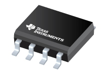
Dual FET Bus Switch With Level Shifting and -2 V Undershoot Protection
Datasheets
SN74CBTD3306C datasheet
PDF, 1.1 Mb, Revision: A, File published: Oct 15, 2003
Extract from the document
Prices
Status
| SN74CBTD3306CD | SN74CBTD3306CDR | SN74CBTD3306CDRE4 | SN74CBTD3306CPW | SN74CBTD3306CPWR | SN74CBTD3306CPWRE4 | SN74CBTD3306CPWRG4 | |
|---|---|---|---|---|---|---|---|
| Lifecycle Status | Active (Recommended for new designs) | Active (Recommended for new designs) | Active (Recommended for new designs) | Active (Recommended for new designs) | Active (Recommended for new designs) | Active (Recommended for new designs) | Active (Recommended for new designs) |
| Manufacture's Sample Availability | No | No | No | No | No | No | No |
Packaging
| SN74CBTD3306CD | SN74CBTD3306CDR | SN74CBTD3306CDRE4 | SN74CBTD3306CPW | SN74CBTD3306CPWR | SN74CBTD3306CPWRE4 | SN74CBTD3306CPWRG4 | |
|---|---|---|---|---|---|---|---|
| N | 1 | 2 | 3 | 4 | 5 | 6 | 7 |
| Pin | 8 | 8 | 8 | 8 | 8 | 8 | 8 |
| Package Type | D | D | D | PW | PW | PW | PW |
| Industry STD Term | SOIC | SOIC | SOIC | TSSOP | TSSOP | TSSOP | TSSOP |
| JEDEC Code | R-PDSO-G | R-PDSO-G | R-PDSO-G | R-PDSO-G | R-PDSO-G | R-PDSO-G | R-PDSO-G |
| Package QTY | 75 | 2500 | 2500 | 150 | 2000 | 2000 | 2000 |
| Carrier | TUBE | LARGE T&R | LARGE T&R | TUBE | LARGE T&R | LARGE T&R | LARGE T&R |
| Device Marking | CC306C | CC306C | CC306C | CC306C | CC306C | CC306C | CC306C |
| Width (mm) | 3.91 | 3.91 | 3.91 | 4.4 | 4.4 | 4.4 | 4.4 |
| Length (mm) | 4.9 | 4.9 | 4.9 | 3 | 3 | 3 | 3 |
| Thickness (mm) | 1.58 | 1.58 | 1.58 | 1 | 1 | 1 | 1 |
| Pitch (mm) | 1.27 | 1.27 | 1.27 | .65 | .65 | .65 | .65 |
| Max Height (mm) | 1.75 | 1.75 | 1.75 | 1.2 | 1.2 | 1.2 | 1.2 |
| Mechanical Data | Download | Download | Download | Download | Download | Download | Download |
Parametrics
| Parameters / Models | SN74CBTD3306CD | SN74CBTD3306CDR | SN74CBTD3306CDRE4 | SN74CBTD3306CPW | SN74CBTD3306CPWR | SN74CBTD3306CPWRE4 | SN74CBTD3306CPWRG4 |
|---|---|---|---|---|---|---|---|
| Additional Features | Powered off protection,-2V undershoot protection,Voltage Level Shifting | Powered off protection,-2V undershoot protection,Voltage Level Shifting | Powered off protection,-2V undershoot protection,Voltage Level Shifting | Powered off protection,-2V undershoot protection,Voltage Level Shifting | Powered off protection,-2V undershoot protection,Voltage Level Shifting | Powered off protection,-2V undershoot protection,Voltage Level Shifting | Powered off protection,-2V undershoot protection,Voltage Level Shifting |
| Bandwidth, MHz | 20 | 20 | 20 | 20 | 20 | 20 | 20 |
| Configuration | 1:1 SPST | 1:1 SPST | 1:1 SPST | 1:1 SPST | 1:1 SPST | 1:1 SPST | 1:1 SPST |
| ESD Charged Device Model, kV | 1 | 1 | 1 | 1 | 1 | 1 | 1 |
| ESD HBM, kV | 2 | 2 | 2 | 2 | 2 | 2 | 2 |
| Input/Ouput Voltage(Max), V | 5.5 | 5.5 | 5.5 | 5.5 | 5.5 | 5.5 | 5.5 |
| Input/Output Continuous Current(Max), mA | 128 | 128 | 128 | 128 | 128 | 128 | 128 |
| Input/Output OFF-state Capacitance(Typ), pF | 5 | 5 | 5 | 5 | 5 | 5 | 5 |
| Input/Output ON-state Capacitance(Typ), pF | 12.5 | 12.5 | 12.5 | 12.5 | 12.5 | 12.5 | 12.5 |
| Number of Channels | 2 | 2 | 2 | 2 | 2 | 2 | 2 |
| OFF-state leakage current(Max), µA | 10 | 10 | 10 | 10 | 10 | 10 | 10 |
| Operating Temperature Range, C | -40 to 85 | -40 to 85 | -40 to 85 | -40 to 85 | -40 to 85 | -40 to 85 | -40 to 85 |
| Package Group | SOIC | SOIC | SOIC | TSSOP | TSSOP | TSSOP | TSSOP |
| Package Size: mm2:W x L, PKG | 8SOIC: 29 mm2: 6 x 4.9(SOIC) | 8SOIC: 29 mm2: 6 x 4.9(SOIC) | 8SOIC: 29 mm2: 6 x 4.9(SOIC) | 8TSSOP: 19 mm2: 6.4 x 3(TSSOP) | 8TSSOP: 19 mm2: 6.4 x 3(TSSOP) | 8TSSOP: 19 mm2: 6.4 x 3(TSSOP) | 8TSSOP: 19 mm2: 6.4 x 3(TSSOP) |
| Rating | Catalog | Catalog | Catalog | Catalog | Catalog | Catalog | Catalog |
| Ron(Max), Ohms | 20 | 20 | 20 | 20 | 20 | 20 | 20 |
| Ron(Typ), Ohms | 3 | 3 | 3 | 3 | 3 | 3 | 3 |
| Supply Current(Max), uA | 1500 | 1500 | 1500 | 1500 | 1500 | 1500 | 1500 |
| Supply Range, Max | 5.5 | 5.5 | 5.5 | 5.5 | 5.5 | 5.5 | 5.5 |
| VIH(Min), V | 2 | 2 | 2 | 2 | 2 | 2 | 2 |
| VIL(Max), V | 0.8 | 0.8 | 0.8 | 0.8 | 0.8 | 0.8 | 0.8 |
| Vdd(Max), V | 5.5 | 5.5 | 5.5 | 5.5 | 5.5 | 5.5 | 5.5 |
| Vdd(Min), V | 4.5 | 4.5 | 4.5 | 4.5 | 4.5 | 4.5 | 4.5 |
| Vss(Max), V | N/A | N/A | N/A | N/A | N/A | N/A | N/A |
| Vss(Min), V | N/A | N/A | N/A | N/A | N/A | N/A | N/A |
Eco Plan
| SN74CBTD3306CD | SN74CBTD3306CDR | SN74CBTD3306CDRE4 | SN74CBTD3306CPW | SN74CBTD3306CPWR | SN74CBTD3306CPWRE4 | SN74CBTD3306CPWRG4 | |
|---|---|---|---|---|---|---|---|
| RoHS | Compliant | Compliant | Compliant | Compliant | Compliant | Compliant | Compliant |
Application Notes
- CBT-C, CB3T, and CB3Q Signal-Switch FamiliesPDF, 584 Kb, File published: Feb 4, 2003
Signal switch devices are widely used in applications requiring bus isolation, multiplexing, demultiplexing, and voltage translation. Compared to other logic and linear product alternatives, signal switches are the fastest and least power consuming. Texas Instruments (TI) CBT-C, CB3Q, and CB3T signal-switch families have low on-state resistance, negligible power consumption, and better undershoot - VOLTAGE LEVEL TRANSLATION (SL) - FamilyPDF, 111 Kb, File published: Sep 21, 2011
- Bus FET Switch Solutions for Live Insertion ApplicationsPDF, 300 Kb, File published: Feb 7, 2003
In today?s competitive computing and networking industry, any equipment downtime due to component interconnects or bus failures impedes communication, hinders productivity and hampers financial growth. In recognizing this increasingly costly unplanned downtime, the industry introduced live-insertion technology to minimize the impact of any such failures. The live-insertion feature enables a networ
Model Line
Series: SN74CBTD3306C (7)
Manufacturer's Classification
- Semiconductors> Switches and Multiplexers> Analog Switches/Muxes
