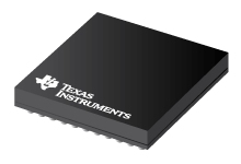
Datasheet Texas Instruments SN74CBTU4411
| Manufacturer | Texas Instruments |
| Series | SN74CBTU4411 |

11-Bit 1-of-4 FET Multiplexer/Demultiplexer 1.8-V DDR-II Switch w/ Charge Pump & Precharged Outputs
Datasheets
SN74CBTU4411 11-Bit 1-of-4 Multiplexer/Demultiplexer 1.8-V DDR-II Switch With Charge Pump and Precharged Outputs datasheet
PDF, 916 Kb, Revision: A, File published: Feb 26, 2016
Extract from the document
Prices
Status
| SN74CBTU4411ZSTR | |
|---|---|
| Lifecycle Status | Active (Recommended for new designs) |
| Manufacture's Sample Availability | No |
Packaging
| SN74CBTU4411ZSTR | |
|---|---|
| N | 1 |
| Pin | 72 |
| Package Type | ZST |
| Industry STD Term | NFBGA |
| JEDEC Code | S-PBGA-N |
| Package QTY | 2000 |
| Carrier | LARGE T&R |
| Device Marking | CTU4411 |
| Width (mm) | 7 |
| Length (mm) | 7 |
| Thickness (mm) | .8 |
| Pitch (mm) | .5 |
| Max Height (mm) | 1.2 |
| Mechanical Data | Download |
Parametrics
| Parameters / Models | SN74CBTU4411ZSTR |
|---|---|
| Additional Features | Pre-charged signal path,Internal pull-down resistors |
| Bandwidth, MHz | 400 |
| Bandwidth(Max), MHz | 334 |
| Configuration | 4:1 |
| ESD Charged Device Model, kV | 0.75 |
| ESD HBM, kV | 2.5 |
| Input/Ouput Voltage(Max), V | 1.9 |
| Input/Output Continuous Current(Max), mA | 100 |
| Input/Output OFF-state Capacitance(Typ), pF | 2.5 |
| Input/Output ON-state Capacitance(Typ), pF | 4.6 |
| Number of Channels | 11 |
| OFF-state leakage current(Max), µA | 10 |
| Operating Temperature Range, C | 0 to 85 |
| Package Group | NFBGA |
| Package Size: mm2:W x L, PKG | 72NFBGA: 49 mm2: 7 x 7(NFBGA) |
| Rating | Catalog |
| Ron(Max), Ohms | 17 |
| Ron(Typ), Ohms | 10 |
| Supply Current(Max), uA | 20 |
| Supply Current(Typ), uA | 2 |
| Supply Range, Max | 1.9 |
| VIH(Min), V | 1.1 |
| VIL(Max), V | 0.66 |
| Vdd(Max), V | 1.9 |
| Vdd(Min), V | 1.7 |
| Vss(Max), V | N/A |
| Vss(Min), V | N/A |
Eco Plan
| SN74CBTU4411ZSTR | |
|---|---|
| RoHS | Compliant |
| Pb Free | Yes |
Application Notes
- Flexible Voltage-Level Translation With CBT Family DevicesPDF, 40 Kb, File published: Jul 20, 1999
Voltage translation between buses with incompatible logic levels can be accomplished using Texas Instruments (TI) translation-voltage clamps (TVC) or standard crossbar technology (CBT) devices. CBT devices in this application offer flexibility in designs, protection of circuits that are sensitive to high-state voltage-level overshoots, and cost efficiency. - 5-V To 3.3-V Translation With the SN74CBTD3384 (Rev. B)PDF, 35 Kb, Revision: B, File published: Mar 1, 1997
The emergence of low-voltage technology required existing 5-V systems to interact with 3.3-V systems. Compatibility issues of mixed-mode operation created the need for 5-V to 3.3-V translation. Buffers and transceivers serve as effective translators. While providing additional drive, these devices also add propagation delay and require directional control. In cases where additional drive is not - 3.3-V to 2.5-V Translation with Texas Instruments Crossbar Technology (Rev. A)PDF, 32 Kb, Revision: A, File published: Apr 3, 1998
- VOLTAGE LEVEL TRANSLATION (SL) - FamilyPDF, 111 Kb, File published: Sep 21, 2011
- Bus FET Switch Solutions for Live Insertion ApplicationsPDF, 300 Kb, File published: Feb 7, 2003
In today?s competitive computing and networking industry, any equipment downtime due to component interconnects or bus failures impedes communication, hinders productivity and hampers financial growth. In recognizing this increasingly costly unplanned downtime, the industry introduced live-insertion technology to minimize the impact of any such failures. The live-insertion feature enables a networ
Model Line
Series: SN74CBTU4411 (1)
Manufacturer's Classification
- Semiconductors> Switches and Multiplexers> Analog Switches/Muxes
