Package Intersil W4x5.20A
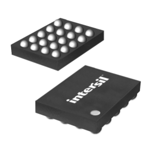
20 Ball Wafer Level Chip Scale Package (WLCSP)
Package Outline Drawing (POD)
Parametrics
| Family | WLCSP-BP |
| Pin Count | 20 |
| Length | 2.34 mm |
| Width | 1.60 mm |
| Height max | 0.53 mm |
| Weight | 0.0040 g |
| Pitch | 0.40 mm |
| Lead Free Peak Temperature | 260 °C |
| Package Index | W4X5.20A |
Model Line
Series: WLCSP (80)
- W11x11.121 W11x11.121A W11x11.121B W13x13.169 W2x2.4 W2x4.8 W3x2.6 W3x2.6C W3x2.6D W3x3.9A W3x3.9B W3x3.9C W3x3.9D W3x3.9E W3x3.9F W3x3.9H W3x4.12 W3x4.12A W3x4.12B W3x4.12C W3x5.15 W3x5.15A W4x3.10A W4x4.16 W4x4.16B W4x4.16C W4x4.16E W4x4.16F W4x4.16G W4x5.20 W4x5.20A W4x5.20B W4x5.20C W4x5.20D W4x5.20E W4x5.20F W4x5.20G W4x5.20H W4x5.20J W4x5.20K W4x5.20M W4x5.20N W4x5.20R W4x5.20S W4x6.24 W4x7.28 W5x5.25 W5x5.25B W5x5.25E W5x5.25G W5x5.25H W5x6.30A W5x6.30C W5x7.28 W5x7.35 W5x7.35C W5x8.40 W5x8.40A W6x6.36 W6x6.36B W6x7.42 W6x7.42B W6x8.48 W6x9.54 W6x9.54A W7x7.49 W7x8.46 W7x8.52 W7x8.56 W7x8.56A W8x12.96 W8x8.64 W8x8.64A W8x9.72 W8x9.72A W8x9.72B W8x9.72C W9x11.99 W9x12.108 W9x9.62
Manufacturer's Classification
- Plastic Packages
