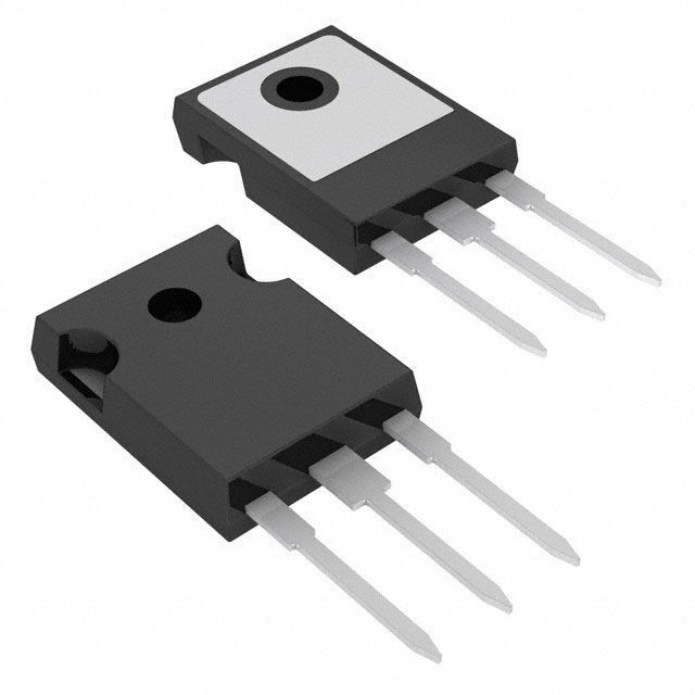
JX0320R065MT3 650V N-Channel MOSFET Description
Silicon Carbide (SiC) MOSFET use a completely new technology that provide superior switching
performance and higher reliability compared to Silicon. In addition, the low ON resistance and
compact chip size ensure low capacitance and gate charge. Consequently, system benefits include
highest efficiency, faster operating frequency, increased power density, reduced EMI, and
reduced system size. Features
High Speed Switching with Low Capacitances High Blocking Voltage with Low RDS(on) Optimized package with separate driver source pin Easy to parallel and simple to drive ROHS Compliant, Halogen free Application
EV Charging Switch Mode Power Supplies DC/DC Converters Power Factor Correction Modules Solar PV inverters Ordering Information
Part Number
JX0320R065MT3 Marking
JX0320R065MT3 1 Package Packaging TO247-3 Tube JX0320R065MT3
Absolute Maximum Ratings(Tc=25℃)
Parameter Symbol
VDS Value Unit 650 V Drain-Source Voltage ID Drain Current(continuous)at Tc=25℃ 8 A ID Drain Current(continuous)at Tc=100℃ 6 A IDM Drain Current (pulsed) 12 A VGS Gate-Source Voltage -8/+18 V PD Power Dissipation TC = 25°C 65 W -55 to +150 ℃ TJ, Tstg Junction and Storage Temperature Range Electrical Characteristics(TJ = 25℃ unless otherwise specified)
Typical Performance-Static
Symbol Parameter Test Conditions BVDS Drain-source Breakdown Voltage ID=250uA,VGS=0V IDSS Zero Gate Voltage Drain Current IGSS Gate-body Leakage Current VGS(th) Gate Threshold Voltage VGSon Recommended turn-on Voltage VGSoff Recommended turn-off Voltage Static Drain-source On Resistance Typ. VDS =0 V ;
VGS =-8 to 18V Static VGS= 15V,ID=2A
TJ= 150°C 2 1.5 Unit
V 50 μA 10 250 nA 1.9 2.5 V TJ=25。C VDS= VGS, ID=1mA Max. 650 VDS =650V, VGS =0V, VGS= 15V, ID=2A
RDS(on) Min. 15 V -3 V 320
500 450 mΩ
mΩ JX0320R065MT3 Typical Performance-Dynamic …