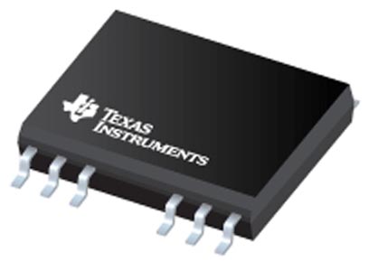
Texas Instruments introduced an isolated dual-channel gate drivers, UCC21320-Q1, with 4-A source and 6-A sink peak current. It is designed to drive power MOSFETs, IGBTs, and SiC MOSFETs up to 5-MHz with best-in-class propagation delay and pulse-width distortion.

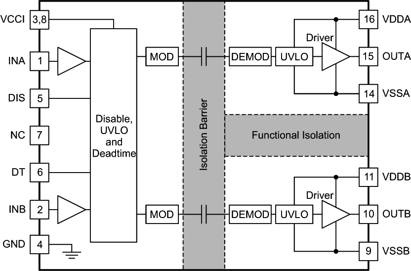
The input side is isolated from the two output drivers by a 3.75-kVRMS basic isolation barrier, with a minimum of 100-V/ns common-mode transient immunity (CMTI). Internal functional isolation between the two secondary-side drivers allows a working voltage of up to 1500 VDC.
 |
| Functional Block Diagram. |
Every driver can be configured as two low-side drivers, two high-side drivers, or a half-bridge driver with programmable dead time (DT). A disable pin shuts down both outputs simultaneously, and allows normal operation when left open or grounded. As a fail-safe measure, primary-side logic failures force both outputs low.
Each device accepts VDD supply voltages up to 25 V. A wide input VCCI range from 3 V to 18 V makes the driver suitable for interfacing with both analog and digital controllers. All supply voltage pins have under voltage lock-out (UVLO) protection.
With all these advanced features, the UCC21320-Q1 enables high efficiency, high power density, and robustness.
 |
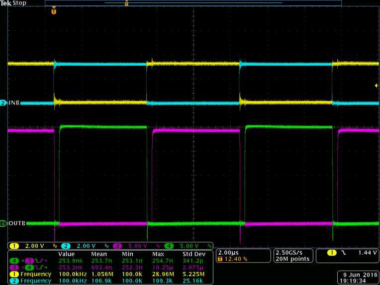
| Bench Test Waveform for INA/B and OUTA/B. |
Features
- 4-A peak source, 6-A peak sink output
- 3-V to 18-V input VCCI range to interface with both digital and analog controllers
- Up to 25-V VDD output drive supply
- Switching parameters:
- 19-ns typical propagation delay
- 10-ns minimum pulse width
- 5-ns maximum delay matching
- 6-ns maximum pulse-width distortion
- Common-mode transient immunity (CMTI) greater than 100 V/ns
- Universal: dual low-side, dual high-side or half-bridge driver
- Programmable overlap and dead time
- Wide Body SOIC-14 (DWK) Package
- 3.3 mm spacing between driver channels
- Operating temperature range –40 to +125 °C
- Surge immunity up to 12.8 kV
- Isolation barrier life >40 years
- TTL and CMOS compatible inputs
- Rejects input pulses and noise transients shorter than 5 ns
- Fast disable for power sequencing
- Qualified for automotive applications
Applications
- HEV and BEV battery chargers
- Isolated converters in DC-DC and AC-DC power supplies
- Motor drive and DC-to-AC solar inverters
- Uninterruptible power supply (UPS)