By Pushkar Ranade
EE Times
For nearly four decades, silicon technology development has been shaped by the growth of the PC industry and the need for continuous improvement in digital transistor performance. A maturing PC industry and a rapidly growing mobile market are changing the dynamics. Will ARM trickle up to high performance, or will Intel trickle down to low power?
The success metrics in the new landscape will be not just higher transistor performance but higher system functionality, smaller system footprint, lower system cost and lower power. These changes will provide opportunities for new players while posing challenges for leading incumbents.
Intel and ARM: CPU vs. SoC
Two competing camps are defining the new landscape. On the one hand is Intel, the leader in silicon process technology and computing architecture (X86). Pitched against the vertically integrated Intel is a lateral ecosystem anchored around ARM, the leader in low-cost/low-power architecture.
While Intel pioneered the era of the CPU, ARM is enabling a massive design and foundry ecosystem, and is ushering in the era of the mobile system-on-chip (SoC). In the CPU space, chip functionality is largely determined by the computing core (for example, Pentium or Athlon), and transistor performance is the critical metric. In the SoC space, the core is just one among a variety of IP blocks that are used to deliver functionality independently.
Intel’s SoC technology has typically been implemented one to two years behind its mainstream technology, which historically has focused on transistor scaling and performance. The foundries within the ecosystem instead focused on integrating disparate functional IP blocks on a chip while also aggressively scaling interconnect density. As the market becomes increasingly driven by low-cost/low-power consumer electronics, and as SoC shipments dominate total silicon volume, one might expect that Intel would look to expand its position in the SoC space.
 |
|
|
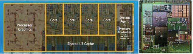
Intel Ivybridge MCU |
SoC NVIDJA Tegra 2 |
Meanwhile, the ARM ecosystem is steadily making inroads into the high-end segment traditionally dominated by Intel. This trend is illustrated by Microsoft’s assertion that its new operating system, Windows 8, is designed for SoC. The predominance of the Intel-Microsoft partnership based on the X86 architecture is coming to an end, as Microsoft’s flagship OS will now run on a wide array of mobile SoC application processors from partners like Qualcomm and Nvidia. The emergence of the SoC era is thus a strategic inflection point for Intel and the ARM ecosystem alike.
Moore’s Law in the SoC era
The semiconductor manufacturing industry is being redefined as the CPU takes a backseat to the mobile SoC. Concurrently, the industry is approaching the limits of technology scaling itself. Eventually, making transistors smaller will result in diminishing returns on key metrics such as performance, power and cost. That will signify another inflection point – when, in the words of Gordon Moore himself, “making things smaller won’t help anymore.”
In a prescient 2001 interview, Moore posited that the inflection point would occur somewhere between 2010 and 2020. As Moore’s Law winds down and the SoC era dawns, the rising influence of the design ecosystem will shape the silicon road map more than the traditional metric of cost per gate. CMOS technology will need to adapt to this changing landscape as it continues to innovate in the new era. Several technology trends indicate a progression toward the inflection point that Moore foresaw.
Transistor leadership
Since the 90-nm generation, Intel has led the way in defining new transistor architecture. Intel’s choice of technology was at times questioned but was ultimately vindicated by the inability of the foundries to deploy an alternative option. At least three waves of innovation support this: silicon on insulator (IBM) vs. bulk (Intel) in the 1990s, biaxial (IBM) vs. uniaxial strain (Intel) in the early 2000s and metal-gate-first (IBM alliance) vs. metal-gate-last (Intel) in the late 2000s.
The metal-gate wave has already changed the contours of the industry, driven by the sheer complexity and cost needed to master it. TSMC began shipping metal-gate technology based wafers in 2011 – nearly four years behind Intel.
The fourth wave of transistor innovation (nonplanar trigate, 2010s) will further shift the landscape. With tri-gate, Intel will significantly widen its lead in transistor performance and complexity.
 |
|
|
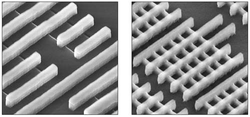
Intel’s nonplanar trigate transistor (right) vs. traditional planar transistor (left). |
Foundries that try to emulate Intel will bear an enormous cost burden in silicon development, tooling and design portability. The foundries also risk an uncertain development timeline, since the compatibility of tri-gate with full SoC integration (digital/analog/passives/RF) remains unknown. Intel not only has the financial might to confront this uncertainty, but it also has the advantage of setting its own design rules for its own architecture and products.
In contrast, the foundries have to support disparate customer needs and may not be able to afford highly restrictive design rules that bloat area density.
Companies that opt to continue using planar technology will face a lesser cost/time burden but will be challenged to innovate as they try to extract superior performance per watt from planar transistors. Tri-gate architecture and the limits of the planar transistor will signify another major inflection point in the CMOS scaling trend.
Ecosystem leadership
Intel’s focus on transistor performance can be traced back to the height of the PC wars, when the benchmark was clock speed. While Intel focused on transistor performance, the foundries adapted Intel’s transistor innovations for their own SoC integration needs. In addition, they aggressively pursued metal density scaling and cost reduction.
While Intel pursued a limited vertical functional integration, the foundries developed a lateral ecosystem and designed transistors for a variety of vendors that independently optimized functionality for each IP block (CPU, GPU, radio, modem, GPS, etc.).
![]()
This vast ecosystem of existing design IP now has a significant influence on the adoption of the next transistor architecture. Arguably, the foundries, though lacking a leading-edge transistor, are today better positioned for the SoC era. TSMC has stated that in 2012 it will integrate a variety of IP blocks and ship highly complex mobile SoC parts to its customers. Those processors will be made in 28-nm technology and will likely set new benchmarks for cost, power and connectivity features.
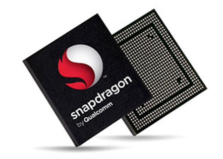
As an example, the Snapdragon processor by Qualcomm might well become the most highly integrated SoC to roll Windows 8 in 2012. Intel has the clear advantage at the transistor level and will win the CPU space, but the ecosystem has the advantage at the system level and is poised to win the SoC space.
‘Making it smaller won’t help’
Geometric scaling of the transistor below a pitch of 80 nm tests the limits of traditional lithography. Innovations such as double or triple patterning and spacer-layer transfer are needed to print features below that pitch. Extremeultraviolet (EUV) patterning has been in development for close to a decade as the successor to 193-nm immersion patterning but remains costly, with limited throughput and ROI.
Since the foundries are ahead of Intel in metal pitch scaling, they will be the first to hit the immersion lithography limit and be required to transition to novel patterning techniques or, ultimately, EUV patterning. Even then, the cumulative cost of patterning will be so high that cost per gate is expected to stay flat or even go up when scaling to the 20-nm node.
It is unlikely the foundries will be able to execute two radical changes – tri-gate and new patterning – within the traditional, two-year development cycle. The 28/20-nm nodes will be very long-lived as foundries grapple with increased cost and complexity in addition to traditional scaling challenges. This will be another inflection point in the morphing of the traditional Moore’s Law metric of cost per gate.
‘Cost per goodness’
In the SoC era, as cost per gate plateaus, the new driver will be “cost per goodness.” Packing as many features (goodness) on a chip as possible at the lowest integrated system cost and power will win. But the cost to design that functionality is also increasing rapidly.
New 28-nm chip designs cost as high as $200 million, up from $100 million for 45-nm designs. While the bulk of the increase is attributed to design complexity, mask costs and embedded software costs are also spiraling.
The transistor architecture that is most compatible with all the IP needs of a complex SoC at the lowest cost will thus have the upper hand. As technology development life cycles get longer and product life cycles get shorter, foundries will try to extract all the goodness in an existing transistor technology before moving to the next one.
This plants the seeds of a paradigm shift. As scaling hits physical and economic limits, the industry will continue to innovate more than ever before. But that innovation will likely be centered on extending the life of an existing geometry, rather than by scaling the geometry itself.