Darvin Edwards
Electronic Design
We’ve come a very long way from the first IC, but we still have a long way yet to go to achieve the full promise of the IC revolution
Sometime in the mid to late 1960s, my father came home excited from the university where he was an assistant professor in the Electronic Technology department. He hustled me into his study, put down his satchel, opened it, and withdrew a small, clear plastic jewel case.
“This is the future of electronics, son,” he said, placing the small box in my hands as though it were a precious treasure. Inside, suspended from black foam by eight or 10 gold plated prongs, was a silvery disk on which rested a tiny grayish sliver of silicon. Fine, barely visible gold strands connected golden posts on the outer edge of the silvery disk to tiny dots on the silicon chip.
I stared at it uncomprehendingly. “What is it?” I asked.
Dad smiled. “It’s an integrated circuit,” he said. “It’s where electronics are going.”
I didn’t know then that I’d be spending over three decades of my life helping improve the capabilities of IC packaging, or that the functionality made possible by integrating transistors on a single substrate would so revolutionize the world in which we live. As I look back, we’ve come a very long way from that early IC. As I look forward, we have a long way yet to go to achieve the full promise of the IC revolution.
Looking Backward: Continuous Change
I joined Texas Instruments (TI) in 1980. There was a crisis. TI had just released its 16k DRAM device, and some customers were finding broken chips in their systems. I was hired to work with a small team chartered to identify the issues causing the die cracking and rectify them. A couple of weeks before I arrived, the team had fabricated its first integrated silicon strain gauge, and I set to work setting up the analysis capabilities and theoretical background that would be needed to characterize and understand the outputs. It was one of the first chip/package interaction test die ever created. Jokingly, one of the managers continuously referred to it as the “strange gauge” chip, rather than the “strain gauge” chip.
The 16 k DRAM went into a 16-pin dual in-line package (DIP). It was the largest die TI had tried to package up to that point, about 5.5 by 3 mm. Using the strain gauge, we quickly identified the impact that mold compounds, molding processes, lead frame design, lead frame downsets, and die attaches were having on the die. We reduced the expansion coefficient and modulus of the mold compound, changed the die attach, eliminated die attach voids, and saw the broken die issue disappear.
Back in the 1980s, packaging was divided along two fronts. One class of packages focused on high-performance, high-power applications. The other catered to consumer products that had neither the performance nor reliability requirements of the compute-intensive applications. The performance category used ceramic materials with cavities. The dies were soldered into the cavities with gold-silicon (AuSi) eutectic before lids were soldered in place, sealing the cavities, forming a hermetic package. These devices were available in either dual in-line configurations or pin-grid area arrays.
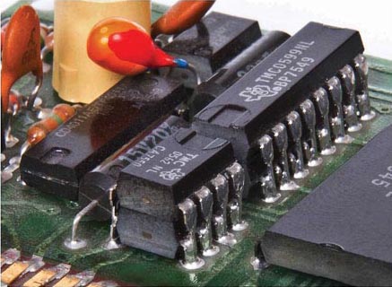
The consumer products were almost exclusively packaged in dual in-line plastic packages. Lots of ingenuity went into getting the most out of the packages. The Figure 1 shows a stacked package concept that was prevalent where two DIP packages were mounted on top of each other, forming an early package-on-package configuration. These devices were also saw-singulated, a technology that is still in use today on no-lead devices.
 |
|
| Figure 1. | This early 1980s “advanced” calculator board included dual in-line packages (DIPs) stacked on top of each other. |
Trends in end product usage and requirements drove needs for improved performance even in the consumer space. The high inductance and capacitance of the DIP approaches made them intractable for high-frequency operation. Additionally, printed-circuit boards (PCBs) were shrinking from sizes suitable for rack-mount to portable product configurations just a couple of inches on a side. This drove the need to reduce pin pitches from the common one-tenth inch (2.54 mm) standard to enable packages to shrink.
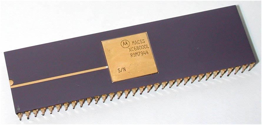
For example, a 64-pin microprocessor package of the early 1980s was almost 3.5 inches long and about 1 inch wide (Figure 2)! Through-hole technology, wherein the leads are inserted through holes drilled in the PCB, simply wouldn’t support the type of pitch needed for this miniaturization. Necessity drove a revolutionary transition to surface mount.
With surface mount, the pins of the package are soldered directly to traces on the PCB rather than being inserted through PCB holes. The pins pitch can be made as fine as the available trace pitch on the PCB and the manufacturing constraints of the lead frames. Solder paste is used to bridge the gap between the package and PCB trace, melting during solder reflow and self-centering the package.
 |
|
| Figure 2. | |
As with any new technology, there were birthing pains. Lead planarity was a killer. All it took to bend the leads was a small bump, and with bent leads, the solder wouldn’t bridge between the lead and PCB land during reflow, leading to opens. An entire sub-industry that built lead-straightening equipment was created to overcome this hassle until the bright idea came to use trays for packing and shipping surface-mount components rather than plastic tubes. Plastic tubes? Yes, tubes were the traditional shipping method for DIP packages, and when surface-mounted packaging started to be developed, they were the default standard. All PCB assembly and test equipment at the time handled tubes. Changing the infrastructure to enable trays took time. In the interim, some unusual package concepts such as J-leaded chip carriers were developed to minimize the planarity issue.
With surface mount came all kinds of component reliability questions. PCB assembly was radically changed. Wave flow soldering transitioned to vapor phase reflow and later IR reflow. Popcorn cracking, or moisture-induced package cracking, became an issue since the entire package is heated during reflow rather than just the leads heating during wave soldering. Solder is not mechanically robust, so temperature-cycling surface-mount components on PCBs started showing solder cracks. Technical conferences began to overflow with papers detailing solder characteristics, board-level reliability testing, methods to overcome moisture damage, and design techniques needed to minimize surface-mount damage.
There were many other issues. Solder inspection was more difficult. The tight pitches on the PCB made the components more susceptible to tin whisker shorting. The tight PCB pitches required tight via spacings, which drove thinner dielectrics. PCB vendors who couldn’t keep up with the tighter pitches lost ground and faded away. New layout tools were required to handle increased complexity as PCBs went from one or two layers thick to upwards of 20 or more layers.
With the increased package density came increased thermal challenges. Power levels of the components were increasing as CMOS was pushed to higher frequencies, and the higher PCB density enabled by surface mount didn’t make thermal management any easier. In the realm of high-performance computing, there was serious talk of 400-W chips becoming commonplace by the early 2000s.
Changing architectures were driving massive needs for increased pins as well. Data buses were moving from 8-bit widths to 16-, 32-, and 64-bit widths, requiring packages that could handle hundreds, and even thousands, of pins. The area array revolution began to meet this need, eliminating the metal pins on the periphery of the devices and replacing them with arrays of solder balls underneath the parts. Metal lead frames gave way to substrates. Wire bonds gave way to flip-chip solder balls. And, small packages began to balloon once again to accommodate the 3000- to 5000-pin requirements of modern telecommunication chip packages.
At the same time, the explosion of portable communications, MP3 players, cell phones, and smart phones pressured the industry to create ever smaller form factors. Wafer chip-scale packages (WCSPs) have become popular to meet these needs, cramming solder balls directly onto the die so the metal interconnection of the die becomes the package itself. Nowadays, the nearly 2000-mm2 package of the 1980s can cover less than 20 mm2 with WCSP technology. And the package miniaturization is continuing, with ever tighter pitches and ever higher pin-counts. It’s not an exaggeration to say that the shrinking form factors of packages have been every bit as important to the electronics revolution as has the relentlessly shrinking transistor.
Looking Forward: It’s Not Finished Yet.
No one has a crystal ball, but some trends are already evident that will drive additional innovation. Implantable devices are beginning to proliferate in ways that will vastly increase as the world demographic ages. Pacemakers, defibrillators, insulin delivery systems, pain blocking regulators, anti-depressant implanted stimulators, Parkinson’s regulators, blood pressure and glucose sensors, artificial retinas, and full body networks with auto-diagnostic capabilities are just a few of the burgeoning medical electronic growth opportunities. These devices will need to operate at microwatt power levels, perhaps scavenging energy from the body itself. Package capacitances will have to shrink even further, and packing densities will need to increase. The body is flexible, and as yet non-mainstream flexible interconnect systems should be a perfect marriage for these applications.
New classes of products, such as automated household assistants, could become as common as cars are today, giving 24-hour support and assistance to this aging population as well as for those who are always on the go and just need some extra household help. These “robots” will be far different from the speculative machines envisioned in iconic science fiction movies, having more limited functionality and not being as anthropomorphic as the Hollywood creations. Instead, in a simpler form factor, they will likely cook, wash clothes, clean dishes, vacuum the floor, and perform any number of other assistive tasks. Electronically enriched, they will drive the need for sensors of all sorts, power electronics to handle tens of precision stepper motors, and computational resources for vision recognition.
The same vision recognition that will enable automated household assistants will also help enable fully autonomous cars. Together with smart, networked roadways, it’s likely that unassisted human driving will become as illegal in the future as drunken driving is today. Or, if populations vote to retain manual driving control, the automotive embedded electronics will at least make the cars as collision avoidant as possible. Some higher-end models sport nascent collision avoidance designs already. As systems become less expensive, as chip and package integration makes them less complex to integrate, they will proliferate.
As I reflect back over my 30-plus year career in packaging, I’m proud to have played a small role in enabling the technologies that have so revolutionized society: the Internet, cheap telecommunications, high-definition TVs, DVRs, gaming systems, ubiquitous computing, GPS navigation, energy-efficient motors, energy-efficient lighting, and all the rest that the IC industry has enabled. Most astonishingly, the revolution has just begun. The best is yet to come.