Haifeng Fan, Texas Instruments
Introduction
The demand for boost regulators has increased recently due to emerging applications in automotive, industrial and consumer marketplaces. Examples of new applications include emergency call (eCall) systems, start-stop systems, audio power amplifiers (PAs), smart grid data concentrators, Thunderbolt™ data ports, power bank for mobile devices, tablet docking stations and many more. In these applications, input power usually comes from low voltage batteries, solar panels, or other low voltage rails, while a higher output voltage is desired. Therefore, a boost (step-up) DC/DC regulator is essential.
Boost power management integrated circuits (ICs) can be configured as either a single-end primary inductance converter (SEPIC) to perform both step-down and step-up (buck and boost), or a flyback regulator to achieve galvanic isolation for enhanced safety and improved noise immunity.
This document explains how to implement boost, SEPIC and flyback regulators with boost power management ICs, and how to choose the right solution. Also covered are approaches to achieve higher output power, improve efficiency, extend input-voltage range, and provide short-circuit protection.
Versatile configurations
Wide VIN boost power management ICs can be configured in various DC/DC topologies to meet different system requirements. The following configurations have in common a low-side control switch.
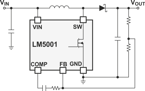
Boost DC/DC regulator
A boost regulator, widely used in low voltage battery-powered systems, provides a higher output voltage than the input. Figure 1 shows the simplified schematic of a boost regulator with the LM5001, high-voltage switch-mode regulator from Texas Instruments (TI). This regulator features an integrated FET which reduces the total solution size.
 |
||
| Figure 1. | Boost regulator with an integrated FET. | |
SEPIC DC/DC regulator
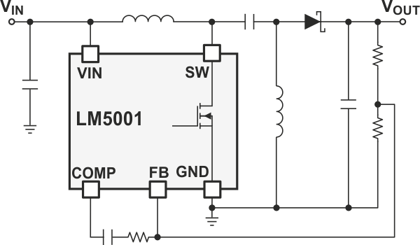
In applications where the input voltage may be either higher or lower than the desired output voltage, a regulator capable of performing both step-down and step-up is required. SEPIC is one of the promising candidates due to its minimal number of active devices and clamped switching waveforms which mitigate electromagnetic interference (EMI). SEPIC, having a low-side control switch in common with the boost regulator, usually is implemented with a boost power management IC. Figure 2 shows a SEPIC regulator using the LM5001, the same IC used in the aforementioned boost regulator example.
 |
||
| Figure 2. | SEPIC regulator with an integrated FET. | |
This schematic shows two separate inductors, which can be a coupled inductor with two windings wound on a common magnetic core to save circuit area.
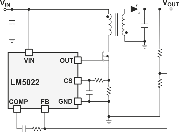
Flyback DC/DC regulator
 |
||
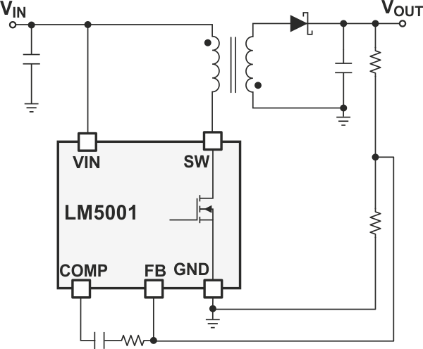
| Figure 3. | Non-isolated flyback regulator with an integrated FET. |
|
Another popular topology using wide VIN boost power management ICs is the flyback regulator, which can be either isolated or non-isolated. A non-isolated flyback regulator (Figure 3) is an alternative solution to SEPIC to realize both step-up and step-down conversion. An isolated flyback regulator (Figure 4) is an attractive solution to provide galvanic isolation, enhanced safety, and improved noise immunity. Besides the simplicity of the flyback regulator, another notable advantage is that no additional magnetic components are required to add multiple outputs.
|
||||||
| Figure 4. | Isolated flyback. | |||||
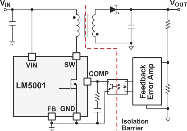
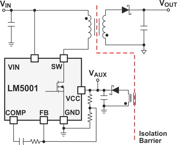
In isolated flyback regulators, either an optocoupler or a tertiary winding is commonly used to implement output voltage feedback. In an isolated flyback with optocoupler, an adjustable shunt regulator such as the LM431, or a standard error amplifier plus a voltage reference, can be employed for feedback from secondary to primary. The design with an optocoupler (Figure 4a) provides tight load regulation for VOUT on secondary side, while the design with a tertiary winding (Figure 4b) features simplicity without additional optocoupler and error amplifier. The output of the tertiary winding (VAUX) also can serve as the bias supply to the regulator to reduce its internal power loss at high VIN.
Choose the right solution
Since there are a wide variety of boost power management ICs, the first question for power supply designers is how to choose the right IC solution for a specific application.
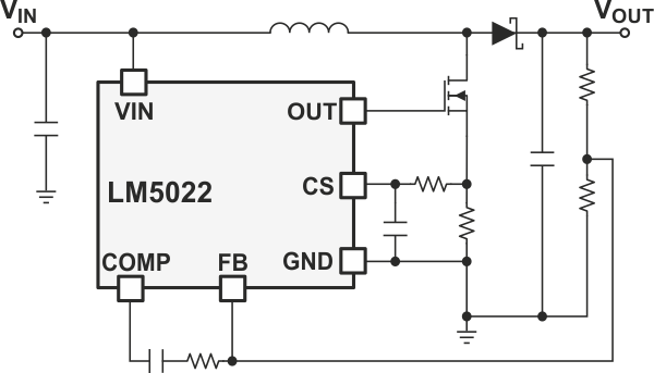
Converter (integrated switch) versus controller (external switch)
TI’s power management IC portfolio includes integrated switch boost solutions called converters, as well as devices requiring external switches called controllers. Converters usually offer higher integration and smaller total solution size. However, converters lack flexibility due to the current and voltage restraints imposed by the integrated switches. For instance, the maximum voltage and peak current of the LM5001’s integrated MOSFET (metal oxide semiconductor field effect transistor) is 75 V and 1A, respectively. Converters are often the preferred choice when an available power management IC supports the voltage and current ratings for the specific application.
 |
||
| Figure 5. | Boost regulator with an external FET. | |
In cases where the required maximum current and/or voltage exceed the capability of boost converters, a boost controller and appropriate MOSFET should be used. Similar to boost converters, boost controllers can be configured as either a boost, SEPIC, non-isolated flyback, or an isolated flyback regulator. Figure 5 and Figure 6 show examples of boost and non-isolated flyback regulators, respectively, designed with the LM5022 controller. Different from converters, controllers give designers freedom to choose appropriate external switches based on their specific needs. The disadvantages are a relatively larger total solution size and a more complicated design.
 |
||
| Figure 6. | Non-isolated flyback with an external FET. | |