Haifeng Fan, Texas Instruments
Non-synchronous versus synchronous rectification
 |
||
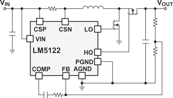
| Figure 7. | Synchronous boost regulator. | |
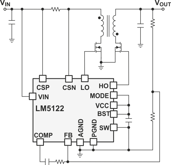
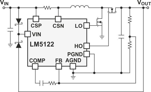
The DC/DC switching regulators shown in the previous examples are all non-synchronous in which a rectifier diode is used. In a synchronous regulator, a MOSFET is used instead. Accordingly, an additional gate driver is required for the synchronous MOSFET. The difference can be better understood by comparing the synchronous boost regulator in Figure 7 with the non-synchronous boost regulator in Figure 5. The LM5022 non-synchronous boost controller only has one low-side gate driver, whereas the LM5122 synchronous boost controller has an additional high-side gate driver for the synchronous MOSFET. The LM5122 also can be configured as a non-isolated synchronous flyback regulator (Figure 8).
 |
||
| Figure 8. | Non-isolated synchronous flyback regulator. | |
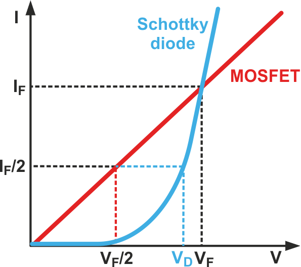
A synchronous recitifier MOSFET usually has lower forward voltage drop than a Schottky diode, which leads to lower conduction loss. Hence, synchronous regulators can obtain higher efficiency, especially in low-voltage and high-current applications. A MOSFET has a positive temperature coefficient of on-resistance, which means the forward voltage drop increases as the temperature goes up. This characteristic causes current to flow equally through multiple devices when they are connected in parallel. As such, a MOSFET is more suitable for parallel operation in high-current applications than Schottky diodes which have a negative temperature coefficient.
Furthermore, paralleling of MOSFETs is much more effective than paralleling of Schottky diodes when it comes to conduction loss reduction. Figure 9 compares parallel operation characteristics between a MOSFET and Schottky diode. Reducing the MOSFET current to half its original value also reduces the MOSFET conduction loss to half its original value due to linear I-V characteristic. In contrast, reducing the Schottky diode current to half its original value also reduces the Schottky loss. However, the new Schottky loss is higher than half its original value because of exponential I-V characteristic.
 |
||
| Figure 9. | Characteristic comparison between MOSFET and Schottky diode. |
|
The main drawback of a synchronous switching regulator is that it requires an additional driver for synchronous MOSFET, which increases the circuit complexity and driving loss. Table 1 is a comparison between synchronous MOSFET and schottky diodes. Designers should chose the solution based on their specific design priorities.
| Table 1. | MOSFET (synchronous) vs. Schottky diode (non-synchronous) | |||||||||||||
|
||||||||||||||
Take your design to the next level
Interleaved multiphase topology for high output power
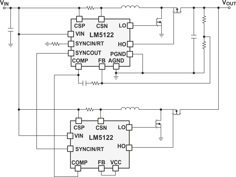
There are a number of ways to handle higher power requirements, of which the interleaved multiphase topology has several advantages. By controlling the phase-shift between the parallel regulators, reduced current ripple, improved efficiency, smaller passive component size, and enhanced thermal performance can be achieved. An interleaved dual-phase synchronous boost regulator with two controllers is outlined in Figure 10. The slave at the bottom is synchronized to a clock generated by the built-in oscillator circuit of the master such that the two phases are 180 degree out-of-phase. The current-sharing between two phases is achieved by current-mode control with a single error amp from the master driving the power stage of both controllers.
 |
||
| Figure 10. | Interleaved dual-phase synchronous boost regulator. | |
DCR sensing for efficiency improvement
The synchronous boost regulator in Figure 7 has an additional current-sense resistor between the input and the inductor in the power path. This current sense resistor generates additional power loss which might be significant in high-current applications.
The boost inductor can be represented as a series combination of an ideal inductor and a lumped direct-current resistance (DCR) (Figure 11). The inherent DCR of the inductor can be used to measure the inductor current which eliminates the discrete current sense resistor and the corresponding power loss. The voltage across the DCR is extracted using a series R-C network in parallel with the inductor. By matching R-C time constant of this network with L/DCR time constant of the inductor, the voltage across the capacitor of R-C network then equals the voltage across the inductor DCR.
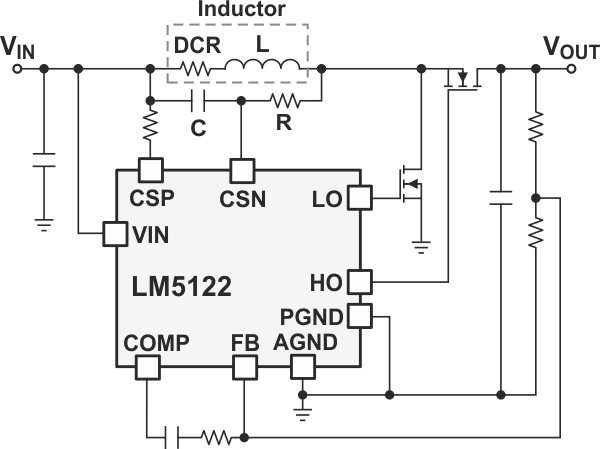 |
||
| Figure 11. | Synchronous boost regulator with DCR sensing. | |
Split-rail configuration to extend input-voltage range
A split-bias-rail configuration, wherein the power stage input and boost IC bias supply are separated from each other, is an effective way to extend the boost regulator input voltage range. For example, the LM5122 requires 3 V of minimum voltage at CSP pin (power stage current sense input) and 4.5 V minimum voltage at VIN pin (IC bias supply). If these two pins are connected as shown in Figure 7, the shared single input (VIN) must be equal to or above 4.5 V to ensure proper operation.
 |
||
| Figure 12. | Split-rail approach extending input-voltage range after start-up. |
|
Figure 12 and Figure 13 present two split-rail configurations. The design in Figure 12 requires a VIN input voltage of 4.5 V or more for start-up. After start-up, VOUT is fed back to VIN as the bias supply via a diode and the regulator maintains normal operation until VIN drops below 3 V. The alternative split-rail approach in Figure 13 uses a charge pump (TPS60150) to produce the VIN bias which, extends the start-up and operating input voltage down to 3 V. This is a notable improvement from the 4.5 V required by the single-rail configuration (Figure 7).
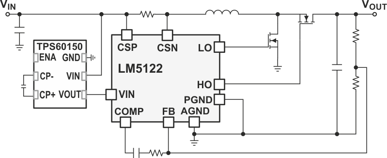 |
||
| Figure 13. | Split-rail approach extending start-up input-voltage range. | |
Load disconnect switch control for short-circuit protection
A basic boost regulator provides no short-circuit protection because the output is connected to the input through the rectifier and inductor when the output is pulled low. Hence, a load disconnect switch is often incorporated to prevent damage from a short circuit. The LM5121 boost design (Figure 14) provides built-in control of the load disconnect switch to provide true short-circuit protection. The additional input MOSFET and gate driver disconnects the output when overload is detected and controls input in-rush current during start-up.
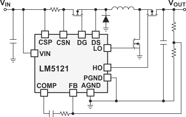 |
||
| Figure 14. | Boost regulator with true short-circuit protection. | |
Conclusion
Wide VIN boost power management ICs can be configured as either a boost, SEPIC, or a flyback regulator to satisfy various application needs. A converter with an integrated switch provides high integration and small total solution size, whereas a controller and external MOSFET offers more flexibility. Non-synchronous solutions feature simple implementation, while synchronous solutions have lower conduction loss and higher efficiency, especially in high-current low-voltage applications. Interleaving, DCR sensing, split-rail, load disconnect switch control provides additional benefits to the boost regulator design. The right solution should be selected based on the specific design requirements and priorities.