This high-efficiency IC with charge pumps and associated circuits reduces input voltage up to one-eighth while providing a 15-W drive for external point-of-load regulators.
Helix Semiconductors’ HS200 DC/DC MuxCapacitor Power IC is a new type of voltage divider that can play an integral role in a distributed power architecture (DPA) system. It provides a high-efficiency approach to reducing the input voltage while delivering a 15-W drive for external point-of-load (POL) converters. To see how the HS200 fits in a DPA system, we first need to look at a typical DPA system.
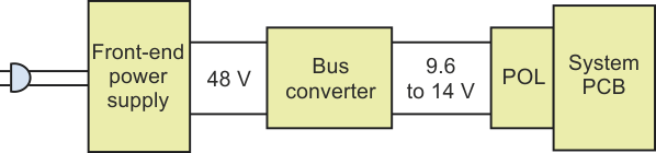
Current DPA systems use a bus converter to deliver an unregulated, stepped-down voltage of 9.6 to 14 V to power a POL (Fig. 1). This bus converter is ideal for a loosely regulated 12-V dc intermediate bus architecture that powers a variety of downstream non-isolated, POL regulators. Both the bus converter and POL are well-suited for applications that use a 48-V (±10%) input bus.
 |
||
| Figure 1. | Shown is one segment of a typical distributed-power-architecture system, which generally incorporates a bus generator. |
|
The HS200 can replace the bus converter by taking the 48-V input and producing a 6-V output to power a POL. Today, POLs produce from 3.3 V to less than 1 V, so 6 V is adequate for most applications.
What is the MuxCapacitor?
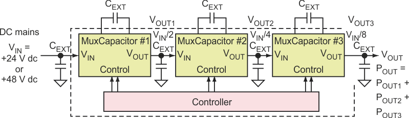
Key to the HS200 is the MuxCapacitor, with its topology that consists of three charge pumps (Fig. 2). Each MuxCapacitor stage can be configured in series to obtain greater voltage division or in parallel for higher current capability. The MuxCapacitor controller optimizes power-delivery efficiency from no-load to maximum power.
 |
||
| Figure 2. | The basic MuxCapacitor voltage-divider configuration includes three charge pumps. | |
The MuxCapacitor employs charge pumps that provide DC/DC voltage conversion using a switch network to charge and discharge two capacitors. The switch network toggles between charge and discharge states of the capacitors. As shown in Fig. 2, above each MuxCapacitor, the "flying capacitor" external CEXT shuttles charge, and the external reservoir capacitor at the output of each charge pump holds the charge and filters the output voltage. Charge-pump modulation (which controls the switch resistance) offers more output current for a given die size (or cost), because it does not need a series pass transistor.
A major advantage of the MuxCapacitor is the elimination of magnetic fields and electromagnetic interference (EMI) that comes with an inductor or transformer. However, one possible EMI source does exist – the high charging current that flows to a "flying capacitor" when it connects to an input source or another capacitor with a different voltage. Although they are electrically simple circuits, MuxCapacitors are capable of end-to-end efficiencies as high as 90-95% at full load, with each stage achieving 99% efficiency in low-current scenarios.
As seen in Fig. 2, you can tap each of the MuxCapacitor outputs to produce three intermediate voltages: VOUT1, VOUT2, and VOUT3. The output of MuxCapacitor #1 is VIN/2, output #2 is VIN/4, and output #3 is VIN/8. Total power drawn from the HS200 cannot exceed 15 W, whereby POUT = POUT1 + POUT2 + POUT3. The integrated multi-stage MuxCapacitor enables a low-profile, high-density IC, where high efficiency reduces thermal loading and lowers packaging costs.
Among the HS200’s features are:
- 63-V maximum input
- Efficiency
- ≥90% at 15 W,
- >97% at 2.5 W
- Operating temperature range of −40°C to 125°C
- Circuit is enabled when EN is high and disabled when EN is low
- 5-mW no-load power consumption
Digging Deeper into the HS200
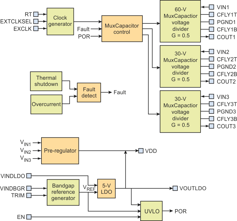
The complete HS200 circuit is shown in Figure 3. The HS200 DC/DC MuxCapacitor IC is an easy-to-use, high-efficiency DC voltage divider. By combining three charge-pump voltage dividers to reduce the input voltage, it allows the use of lower voltage/lower cost POL regulators or other power converters.
 |
||
| Figure 3. | This block diagram of the HS200 shows the associated circuits to control the MuxCapacitor. | |
Each HS200 MuxCapacitor Voltage Divider (MCVD) uses an external flying capacitor, an internal switching circuit, and an external reservoir capacitor. The switching device is configured to operate the corresponding voltage-reduction circuit at charging and discharging phases from a two-phase, non-overlapping, on-chip clock generator. A soft-start current-limiting input switch with high RDS(ON) is used for the first-stage MCVD to limit the in-rush current when the IC is first enabled.
Each MuxCapacitor IC contains overcurrent protection that automatically resets once the overcurrent condition clears. This feature is active at startup, enhancing a soft-start ramp-up at each VOUT.
The VINLDO pin powers a low-power bandgap reference generator. The bandgap circuit includes a temperature-compensated output voltage used as a reference by the internal sub-circuit blocks. The bandgap incorporates a startup circuit and is always on even when enable is low.
The integrated 5-V LDO powered from the VINLDO pin provides the supply voltage for the analog circuits. It uses the bandgap output as the reference voltage to generate the desired output voltage. This LDO includes short-circuit protection and is always on even when enable is low.
An undervoltage-lockout (UVLO) circuit monitors the voltages at the 5-V LDO output and the Enable pin. It ensures that the MuxCapacitor outputs remain in the off state whenever one of these signals drop below the set thresholds. Normal operation resumes once the signals rise above their thresholds.
The HS200 generates a Power On Ready (POR) signal when each signal reaches its valid logic level. When the POR is asserted, the soft-start sequence starts. All UVLO comparators except for the enable circuit are disabled when enable is low, which provides ultra-low power dissipation.
Clock Generator
An external 400-kΩ resistor (typical) connected from the RT pin to GND programs the integrated clock generator’s switching frequency of 100 kHz. Using the EXTCLK pin, you can synchronize this clock signal to an external clock. Switching activity at the EXTCLK pin enables the internal synchronizer. When the synchronizer is enabled (EXTCLKSEL = 1), the MuxCapacitor clock tracks the EXTCLK pin switching rate. As the EXTCLK pin frequency slows down, the MuxCapacitor clock slows down. The EXTCLK signal is derived from the external power converter’s switch drive signal. This allows the MuxCapacitors to save power, because the external switcher slows down due to reduced load demand.
An over-temperature detector, with its trip threshold set to 145͘͘ °C, accepts over-temperature sensing signals. The thermal shutdown threshold has 20°C hysteresis. If the trip threshold is exceeded, thermal shutdown turns off the MuxCapacitor outputs and resets the internal soft-start. Restart is initiated automatically when the sensed temperature drops down within the normal operating range. The thermal shutdown is disabled when enable is low, which enables ultra-low power dissipation.
 |
||
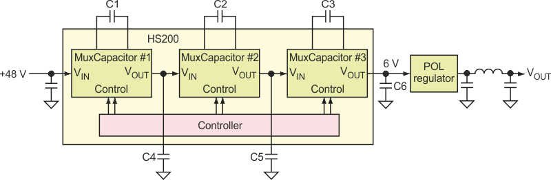
| Figure 4. | The HS200 reduces the 48-V in to 6 V to power the external POL regulator. C1, C2, and C3 are external “flying capacitors,” and C4, C5, and C6 are external reservoir capacitors. |
|
Figure 4 shows a simplified diagram of the HS200 reducing the 48-V input to 6 V, which powers an external POL regulator. The VOUT3 output voltage provides the VIN for the POL regulator. This configuration maximizes the regulator efficiency.