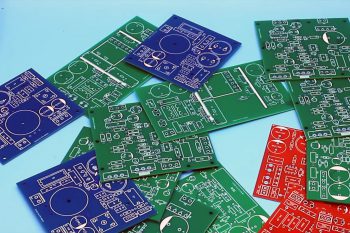
The PCB production process is not a secret for people who once used to make them at home conditions. It's time to check the production process of creating a printed circuit board looks like on a huge scale. All on the example of one of the JLCPCB factory – the largest manufacturer of prototype PCBs in China. The company is able to carry out around 10,000 orders per day, which translates into over 400,000 square meters of PCB every month. But they always keep special offer – $2 for 10 pcs PCBs (2-layer, 100×100 mm) on https://jlcpcb.com.
The process described below applies to a 2-layer PCB, the most popular among hobbyists. The PCB production process with more layers varies in sequence and number of stages. Some are carried out several times, and additionally there is a process of "gluing" further layers of copper and insulating spacers in special presses.
 |
| Despite the high level of automation, people are still needed in PCB paints. |
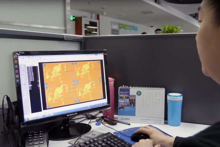
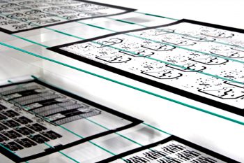
1. Overview of project files
After designing the PCB in our program, the key step is to create files commonly referred to as "Gerber". It is a collection of formats that describe our project in a way understandable to machines and greatly facilitate the work of people preparing production. They also allow you to immediately notice potential problems thanks to comparisons to device limitations. Although the verification is largely done automatically, most often we have an engineer on the other side, which will draw our attention when, for example, the tracks are too close to each other, the grommets are too small in diameter, or the descriptive layer overlaps the solder pads. In case of small problems, the engineer himself can propose an amendment and ask us for approval. If the problems are more serious, the project will be rejected, and the files need to be corrected by ourselves.
 |
| PCB design verification. |
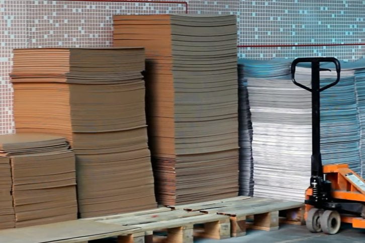
2. Preparation of the laminate
Almost every PCB factory has its own warehouse in which it holds piles of laminates with different dimensions and parameters. Laminates may differ, for example, in the thickness of copper, the thickness of the insulating layer, and even the material with which the layer is made. Sheets are often jagged and uneven, so one of the first steps is to cut them and clean them. The edges are polished, secured and the laminate travels to the next part of the factory.
 |
| Laminate sheets ready for pre-treatment. |
3. Drilling
The sheet goes to special numerical drills. Smaller mounting holes, holes for future grommets, as well as special openings to facilitate positioning of elements in later stages of production are made. Each drill has a set of drills of various diameters and it changes them autonomously depending on the requirements given in the design files. After drilling, the sheets are cleaned of residual material and the copper surface is gently ground to get rid of furrows and scratches.
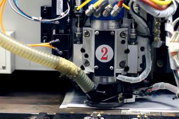 |
| CNC drilling machine. |
| |
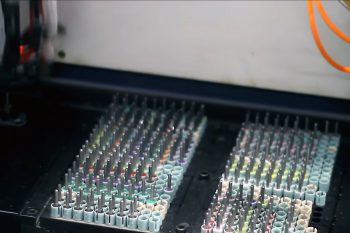 |
| Modules of exchangeable drills. |
4. Metallization
This stage forms a thin shell of copper, among others in the holes to be metalized. At the JLCPCB factory, this is achieved by immersing the drilled laminate in a special chemical bath. Due to the metallization of the openings, it is possible to make vias connecting the copper layers in a manner consistent with our design. After removing the sheet from the bath, it is thoroughly rinsed and dried.
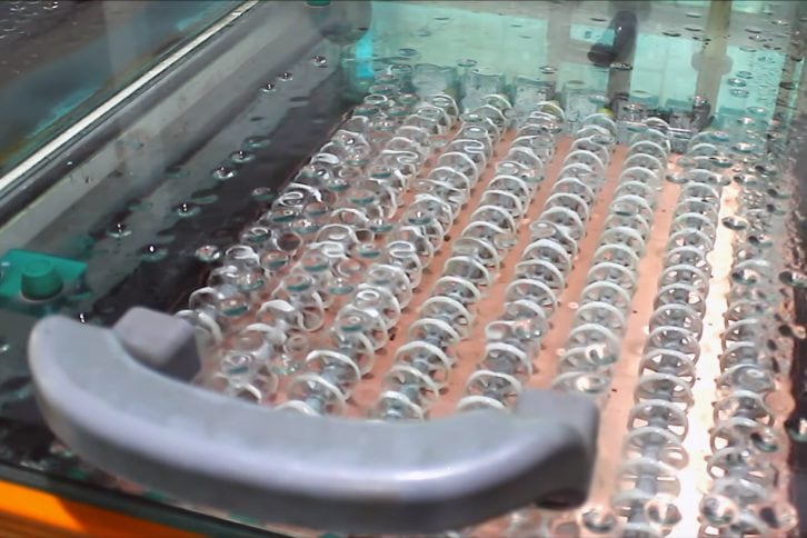 |
| Chemical bath – pre-metallization of holes. |
5. Applying a photosensitive layer
A special photosensitive layer is applied on the copper side of the laminate. The layer in the form of a foil is glued on the laminate, and on it is put on special masks, i.e. transparent plates with printed paths from our project. The "sandwich" created in this way is placed under a UV lamp whose light cures a part of a photosensitive film with an unshielded mask. The laminate is then thoroughly cleaned of the uncured photosensitive layer, and then dried and preheated in an oven. As a result, the hardened layer becomes mechanically more resistant.
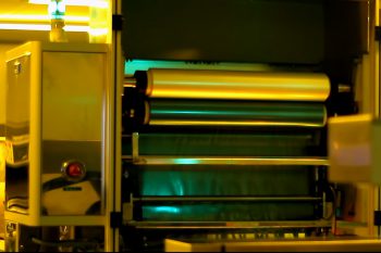 |
| Roll with light-curing foil. |
| |
 |
| UV mask with a path outline. |
6. Tin coating
The laminate is covered with a tin coating - the light-cured part of the copper, unprotected by the hardened layer, and metallized holes are covered with a thin layer of metal similar to the popular solder binder. This is usually achieved by immersing the laminate in a special ladle of molten SnPb alloy, and when drawing out, special air nozzles blow off its excess from the surface of the sheet. Then the plate is melted in another chemical bath, which is designed to dissolve and remove the photosensitive coating. The process is repeated several times until copper from this coating is completely exposed.
 |
| PCB during metallization of exposed copper fields. |
| |
 |
| PCBs with metallized copper fields. |
7. "Digging" of copper
The next chemical process is crucial because it forms the PCBs' paths and pads. The copper unprotected in the previous stages is removed from the laminate thanks to a special solution similar to the popular B327, which is applied by special nozzles. After removing the copper, the process of removing the previous tin coating takes place – a special chemical bath reveals paths and pads of pure copper.
 |
| Etched PCB with copper still covered with tin. |
| |
 |
| Transport of etched PCBs. |
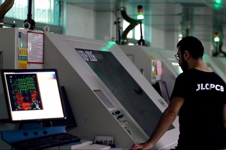
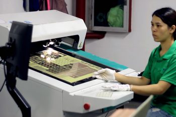
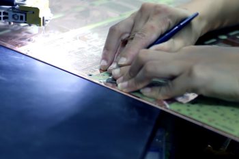
8. Quality control and corrections
Sheets are checked by an advanced vision system supported by an employee equipped with various chisels and scrapers. After detecting the differences between the appearance of the tile and the project file, the person supervising the process decides whether the defect is serious and the tile must be discarded (eg, over-etching), or the tile can be repaired manually (eg, not). Repair is usually done under powerful microscopes, so the effect is often satisfactory.
 |
| The computer vision system checks PCB compatibility with the design. |
| |
 |
| Small errors are improved by hand. |
9. Solder mask
The process of applying a protective mask can have two variants. The first uses a technique similar to screen printing, where a special polymer paint is spread by a special template (covering eg soldering pads). The second variant is more complicated, but more precise. Requires a soldermask layer that has light-curing properties. Masks on transparent plates, curing with UV lamps are again used and the uncured mask is removed during the chemical bath. The next stage is the process of heating and cooling, the purpose of which is to harden the soldermask coating, thanks to which it protects better the copper underneath and gains better parameters as an electrical insulator.
 |
| Special machines rotate double-sided plates. |
| |
 |
| Solder masks can have different colors. |
10. Descriptive layer
Two options are also foreseen at this stage. The first covers large production series, in which speed counts. A special template is laser cut and used to apply paint in a manner analogous to the screen printing technique. If the series is small and the production of the template becomes unprofitable, the second option is chosen and a special "printer" that prints the descriptive layer on the laminate.
 |
| A template used to apply a descriptive layer. |
| |
 |
| The appearance of the PCB with a descriptive layer. |
11. Coating
Because copper oxidizes very quickly in contact with air, it is protected with a metallized coating. More expensive options allow the use of technical gold, which has great parameters as a guide and solder well, while a slightly cheaper option is the usual coating of tin (SnPb), which probably each of us had the opportunity to meet. It gives the pads a characteristic "silver" color.
 |
| Sheets of PCBs with a copper coating against oxidation. |
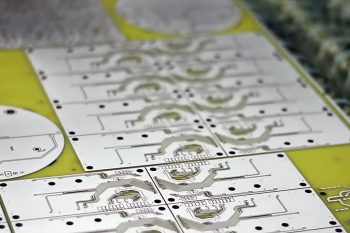
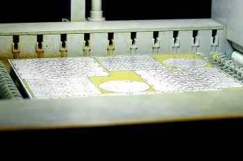
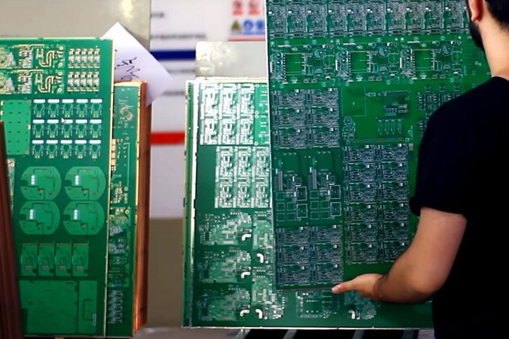
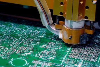
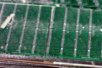
12. Cutting and milling
Until then, all processes were performed on a huge laminate sheet. One sheet can contain many PCBs in its area, and they are often of different designs. Such sheets are processed in special numerical milling machines that cut out larger openings, separate designs from each other or lightly cut PCB panels (so-called V-groove), thanks to which we can easily separate them later.
 |
| CNC milling head. |
| |
 |
| Cut PCB panels. |
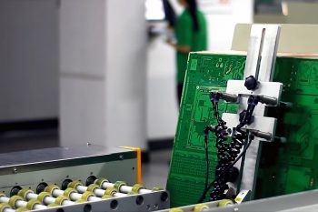
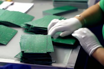
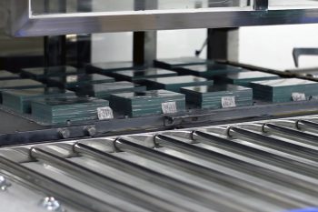
13. Testing
The tiles are placed in special tripods, and simple robots quickly check the quality of electrical connections and their compatibility with the design. At the end, they are once again viewed by the quality control department supported by computer vision, converted by the employee, packed in vacuum and transported to the dispatch department.
 |
| Automatic testing machine for electrical connections. |
| |
 |
| Inspection and counting of made PCBs. |
| |
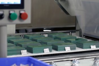 |
| PCB stack ready to be packed. |
| |
 |
| Order packed vacuum in heat-shrinkable foil. |
| |
PCB production process can be seen in the following video from the JLCPCB factory. Some of the stages are covered by the secret, but most of the basic activities have been presented very carefully: