There are standard techniques to generate negative output voltages, and there are well-known approaches to dynamically adjust an output voltage. The missing link that I hope to address in this article combines both techniques with a simple level-shifting circuit.
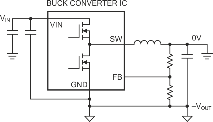
Applications that require power supplies with negative output voltages include test and measurement, aerospace and defense, automotive, and medical. One common approach to creating a negative power rail is to use a conventional buck converter but operate it as an inverting buck-boost converter (References 1-3). The buck converter integrated circuit (IC) ground pins connect to the negative output voltage node (–VOUT) and the inductor output connects to system ground (0V). Figure 1 is an example configuration. The resistor divider from the output to the feedback pin sets the output voltage.
 |
||
| Figure 1. | Operating a buck converter as an inverting buck-boost converter generates a negative output voltage. |
|
A key challenge with generating a negative voltage using a buck converter IC is how to interface and level-shift signals to and from the IC. The input/output (I/O) pins are referenced to the negative output voltage (–VOUT) instead of to system ground (0V). TI’s application report [4] does a great job explaining several circuits that level shift the enable (EN), power good (PGOOD), and synchronization (SYNC) signals between the system ground (0V) domain and the local IC ground (–VOUT) domain. The report also includes useful suggestions on how to test the circuit by measuring Bode plots and load transient response. Another application report [5] also includes some level-shifting circuit examples.
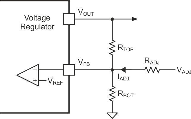
Next, let’s examine dynamic voltage adjustment. For a conventional buck or boost converter, References [6, 7, and 8] demonstrate several methods to adjust the output voltage. One popular method uses a resistor connected between the FB pin and an adjustable voltage source (VADJ), as shown in Figure 2. The voltage at VADJ is adjusted up or down to dynamically adjust the converter’s output voltage. Current will flow through resistor RADJ into the FB node when VADJ is higher than the FB node voltage (which equals the reference voltage, VREF). This results in the output voltage decreasing.
 |
||
| Figure 2. | You can dynamically adjust a converter’s output voltage by sourcing/ sinking current into the FB node. |
|
Conversely, if the VADJ voltage is lower than the FB node voltage, current will flow in the opposite direction across resistor RADJ and the output voltage will increase.
One way to think about it is that the sourcing (or sinking) current into the FB node makes it appear like the top (or bottom) resistance value has decreased. The resistor’s RADJ acts like a virtual resistor in parallel with the top or bottom resistor.
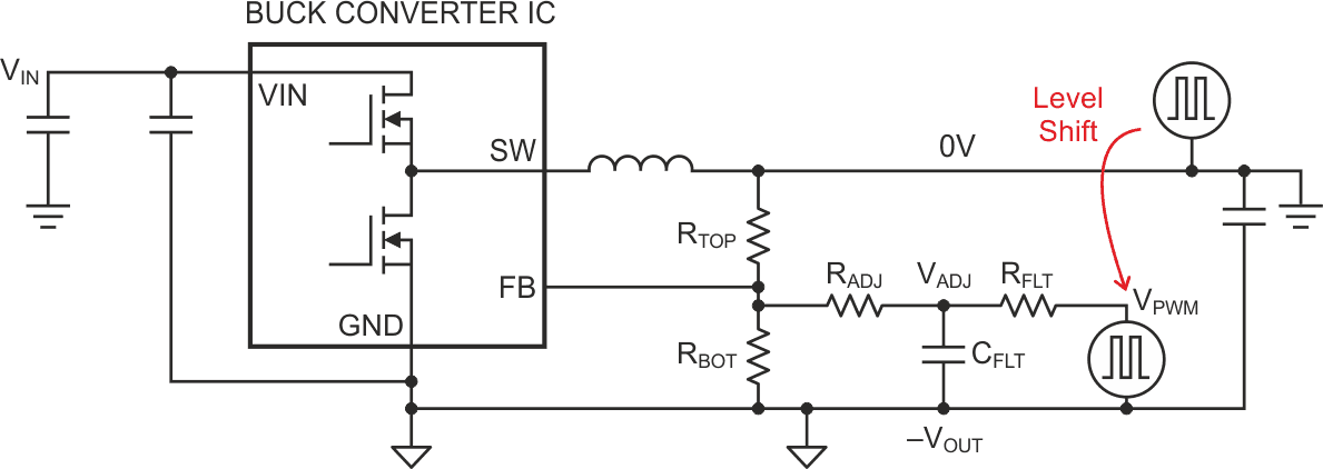
One simple approach to generating VADJ is to provide a pulse-width modulation (PWM) signal that passes through a resistor-capacitor low-pass filter. A microcontroller or other digital chip can output the PWM signal. Controlling the PWM signal’s duty ratio will change VADJ. Using this approach to dynamically adjust the negative output voltage of an inverting buck-boost converter can be a difficult task because the buck converter IC’s local ground is riding on the negative output voltage (–VOUT) instead of the system ground (0V). Level-shifting circuits will likely be necessary, like the interfacing of I/O pins that I mentioned earlier (Figure 3).
 |
||
| Figure 3. | Using a ground referenced PWM signal to generate VADJ requires a level-shifting circuit. | |
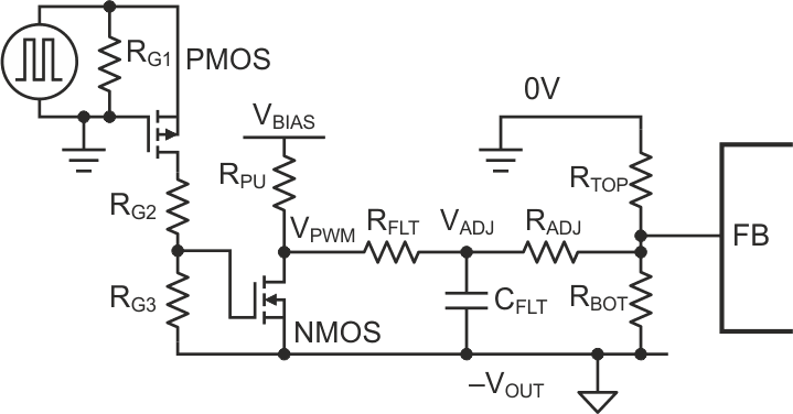
Figure 4 shows an example level-shifting circuit for this application. This circuit will convert a PWM signal that is with respect to system ground (0V) to a PWM signal that is with respect to the IC ground (–VOUT). The PWM source turns the P-channel metal-oxide semiconductor field-effect transistor (MOSFET) on and off. When the P-channel MOSFET turns on, it pulls the N-channel MOSFET gate above the gate’s threshold voltage and turns the N-channel MOSFET on. In turn, this pulls VPWM low to –VOUT. When the P-channel MOSFET turns off, the N-channel MOSFET turns off and resistor RPU pulls VPWM up toward VBIAS. VBIAS can be generated using a precision shunt regulator, such as the Texas Instruments LM4040, which is connected to VIN through a resistor and to –VOUT. As shown in Figure 3, RFLT and CFLT act as a low-pass filter and create VADJ. The current through RADJ will adjust the output voltage.
 |
||
| Figure 4. | This example level-shifting circuit uses discrete components to convert the PWM signal from ground reference to the IC’s reference, –VOUT. |
|
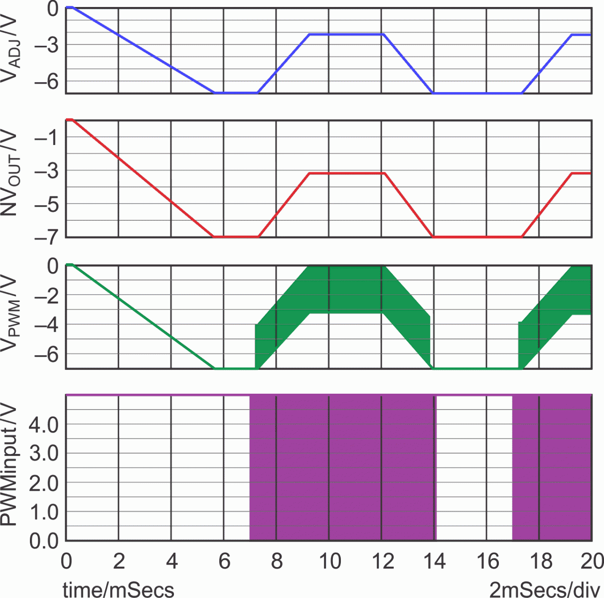
The simulation results in Figure 5 show this approach’s ability to adjust a negative output voltage, with a buck converter operating as an inverting buck-boost converter. During the first 6 milliseconds (ms), the negative output voltage (shown in red and labeled “NVOUT”) starts softly to –7 V. The blue line shows VADJ, which tracks the negative output voltage during startup. The PWM circuit is enabled at 7 ms (the PWM input waveform is shown in purple) and generates the level-shifted PWM (VPWM). VADJ (shown in blue) increases, and the converter output voltage increases in response. The converter reaches the new steady-state operating point (near –2 V) after about 2 ms of transition time. Adjusting the PWM signal lowers the output voltage later in the simulation, with smooth, effective results.
 |
||
| Figure 5. | Simulation shows how a level-shifting circuit can be used to dynamically adjust a negative output voltage. |
|
Using a simple circuit to enable an adjustable negative output voltage can work with many off-the-shelf buck converter ICs. This circuit combines common techniques for adjusting the output voltage and level shifting signals. The level-shifting circuit presented here enables a system ground-referenced PWM source to change the current injected into the power converter’s FB node. The key design challenge is controlling this injected current while the local IC ground voltage (which is at the same voltage potential as the negative output voltage) changes. This technique is suitable for various applications that require the dynamic adjustment of a negative output voltage.
References
- Tucker, John, “Using a buck converter in an inverting buck-boost topology,” Analog Design Journal SLYT286, 4Q07.
- Tucker, John, “Using the TPS5430 as an Inverting Buck-Boost Converter,” Texas Instruments application report SLVA257A, August 2007.
- Daniels, David G, “Create an Inverting Power Supply From a Step-Down Regulator,” Texas Instruments application report SLVA317B, February 2009.
- Frank De Stasi "Working with inverting buck-boost converters," Texas Instruments application report SNVA856, February 2019.
- Anthony Fagnani, Alexander Bernussi “Level-Shifting Control for an Inverting Buck-Boost,” Texas Instruments application report SLVA540, January 2013.
- Texas Instruments 30-V to 150-V Adjustable Output Voltage Boost Reference Design for LIDAR Applications, 2018.
- “How to Dynamically Adjust Power Module Output Voltage,” Texas Instruments application report SLVA861, December 2016.
- Glaser, Chris, “Methods of output-voltage adjustment for DC/DC converters,” Analog Design Journal SLYT777, 3Q19.