Designing astable circuits using the industry-standard 555 timer is a straightforward process when duty cycles are 50% or greater. However, you must overcome the many pitfalls of low-duty-cycle circuits to arrive at a desired result. Using only ideal components eases the design, but the components themselves are hard to obtain. Nonideal components get in the way of the easy-to-use standard equations and greatly multiply the tolerances. This Design Idea uses the TLC555 CMOS timer. You can use other versions of the popular 555 timer with appropriate variations in the given parameters. For a standard, greater-than-50%-duty-cycle, low-frequency design (Figure 1), you would use the following design equations:
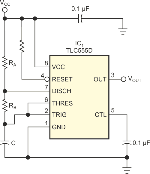 |
||
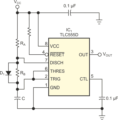
| Figure 1. | This classic 555-based timer is valid only for duty cycles greater than 50%. |
|
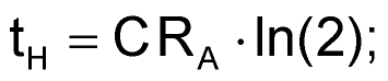
Charging current for the timing capacitor flows through RA and RB until the capacitor voltage reaches the upper threshold voltage of 0.667VCC. The capacitor then discharges through RB and an internal transistor to the lower threshold voltage of 0.333VCC. Because RB is present in both the charging and the discharging cycles, you can’t implement duty cycles lower than 50% in this configuration. These idealized equations also ignore several factors that slightly degrade the results for the higher range of duty cycles but greatly influence the results of low-duty-cycle designs. These factors include propagation delays and the on-resistance of the internal discharge transistor. All these factors are supply-voltage-dependent. Another factor for low-duty-cycle designs that does not apply to high-duty-cycle designs is the effect of the RB bypass diode, D1 (Figure 2), required to implement the design.
 |
||
| Figure 2. | The simple addition of a bypass diode makes this timer circuit valid for low duty cycles. |
|
Adding a bypass diode across RB allows for designs with duty cycles lower than 50%. During the charging cycle, current flows through RA and bypasses RB through the diode. During discharge, current flows through RB and the internal discharge transistor as usual. Because RB is now present only in the discharge cycle, you can tailor the duty cycle to any desired point over the full range. Again, using ideal components, the timing equations are simple:

The factors you must consider in obtaining a design that agrees with calculations include the:
- diode forward voltage,
- propagation delays,
- discharge-transistor on-resistance,
- ratio of RA to on-resistance, and
- leakage resistance of the control-pin capacitor.
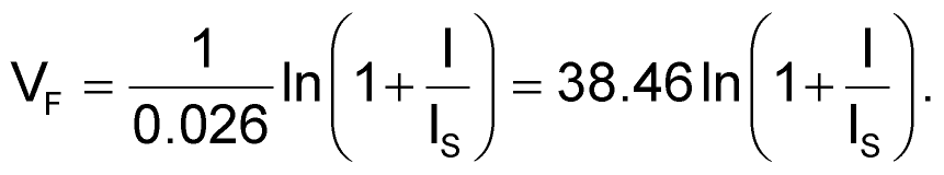
Diode forward voltage depends on the current flowing through the diode. This current can range from a few hundred microamps to tens of milliamps. For a fixed design, you can obtain this voltage from manufacturers’ curves or actual measurements you make by applying the desired current through the diode. You can also use the diode equation:

Or, in terms of voltage:
This voltage subtracts from the charging voltage during the charging cycle and affects the charge-ramp time. Propagation-delay times from the THRES (threshold) and TRIG (trigger) inputs to DISCH (discharge) add directly to the period. These delays depend upon supply voltage. The formulas for the propagation delays (in nanoseconds) are:


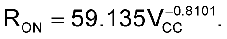
Discharge-transistor on-resistance also varies with supply voltage. This resistance affects the discharge current. Also, when you use low-value resistors for RA (for low-duty-cycle designs), the combination of RA and the on-resistance yields a voltage divider that affects the discharge voltage. The on-resistance formula for resistance in ohms is:
Typically, you’d place a small capacitor on the control pin that connects to the upper internal-divider node. This capacitor has only a slight effect on the threshold-trigger voltages. The leakage resistance of the ceramic capacitor is approximately 9 MΩ. This value is high but still accounts for approximately a 1.5% drop in the trigger voltages because of the 80-kΩ divider resistors that the window-comparator circuit uses. When you take all the cited parameters into account, the design equations become considerably more complicated:
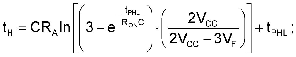
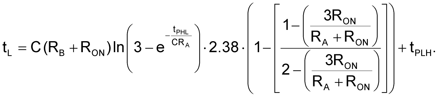
These equations include all the known parameters to obtain a nominal design using the TLC555 timer. Tolerances in each of the parameters cause additional variations that you must consider. In addition, you must consider the effects of temperature variations. After you obtain all this knowledge, the simple 555 timer presents a major math problem. However, thanks to modern computers, you can eliminate much of this tedious math using an Excel spreadsheet. It shows the results of calculations both with and without the bypass diode and includes the tolerancing parameters. You can download the spreadsheet by clicking on the link in the Downloads section.