Ground Plane
There is much more to discuss than can be covered here, but we’ll highlight some of the key features and encourage the reader to pursue the subject in greater detail. A list of references appears at the end of this article.
A ground plane acts as a common reference voltage, provides shielding, enables heat dissipation, and reduces stray inductance (but it also increases parasitic capacitance). While there are many advantages to using a ground plane, care must be taken when implementing it, because there are limitations to what it can and cannot do.
Ideally, one layer of the PCB should be dedicated to serve as the ground plane. Best results will occur when the entire plane is unbroken. Resist the temptation to remove areas of the ground plane for routing other signals on this dedicated layer. The ground plane reduces trace inductance by magnetic-field cancellation between the conductor and the ground plane. When areas of the ground plane are removed, unexpected parasitic inductance can be introduced into the traces above or below the ground plane.
Because ground planes typically have large surface and cross-sectional areas, the resistance in the ground plane is kept to a minimum. At low frequencies, current will take the path of least resistance, but at high frequencies current follows the path of least impedance.
Nevertheless, there are exceptions, and sometimes less ground plane is better. High-speed op amps will perform better if the ground plane is removed from under the input and output pads. The stray capacitance introduced by the ground plane at the input, added to the op amp’s input capacitance, lowers the phase margin and can cause instability. As seen in the parasitics discussion, 1 pF of capacitance at an op amp’s input can cause significant peaking. Capacitive loading at the output – including strays – creates a pole in the feedback loop. This can reduce phase margin and could cause the circuit to become unstable.
Analog and digital circuitry, including grounds and ground planes, should be kept separate when possible. Fast-rising edges create current spikes flowing in the ground plane. These fast current spikes create noise that can corrupt analog performance. Analog and digital grounds (and supplies) should be tied at one common ground point to minimize circulating digital and analog ground currents and noise.
At high frequencies, a phenomenon called skin effect must be considered. Skin effect causes currents to flow in the outer surfaces of a conductor – in effect making the conductor narrower, thus increasing the resistance from its dc value. While skin effect is beyond the scope of this article, a good approximation for the skin depth (D) in copper, in centimeters, is
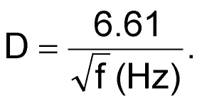 |
(5) |
Less-susceptible plating metals can be helpful in reducing skin effect.
Packaging
Op amps are typically offered in a variety of packages. The package chosen can affect an amplifier’s high-frequency performance. The main influences are parasitics (mentioned earlier) and signal routing. Here we will focus on routing inputs, outputs, and power to the amplifier.
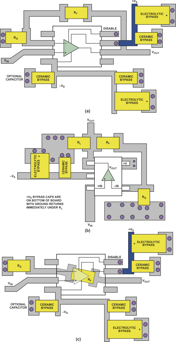
Figure 9 illustrates the layout differences between an op amp in an SOIC package (a) and one in an SOT-23 package (b). Each package type presents its own set of challenges. Focusing on (a), close examination of the feedback path suggests that there are multiple options for routing the feedback. Keeping trace lengths short is paramount. Parasitic inductance in the feedback can cause ringing and overshoot. In Figures 9(a) and 9(b), the feedback path is routed around the amplifier. Figure 9(c) shows an alternative approach – routing the feedback path under the SOIC package – which minimizes the feedback path length. Each option has subtle differences. The first option can lead to excess trace length, with increased series inductance. The second option uses vias, which can introduce parasitic capacitance and inductance. The influence and implications of these parasitics must be taken into consideration when laying out the board. The SOT-23 layout is almost ideal: minimal feedback trace length and use of vias; the load and bypass capacitors are returned with short paths to the same ground connection; and the positive rail capacitors, not shown in Figure 9(b), are located directly under the negative rail capacitors on the bottom of the board.
 |
||
| Figure 9. | Layout differences for an op-amp circuit. (a) SOIC package, (b) SOT-23, and (c) SOIC with RF underneath board. |
|
Low-distortion amplifier pinout: A new low-distortion pinout, available in some Analog Devices op amps (the AD8045, for example), helps eliminate both of the previously mentioned problems; and it improves performance in two other important areas as well. The LFCSP’s low-distortion pinout, as shown in Figure 10, takes the traditional op amp pinout, rotates it counter-clockwise by one pin and adds a second output pin that serves as a dedicated feedback pin.
 |
||
| Figure 10. | Op amp with low-distortion pinout. | |
The low-distortion pinout permits a close connection between the output (the dedicated feedback pin) and the inverting input, as shown in Figure 11. This greatly simplifies and streamlines the layout.
 |
||
| Figure 11. | PCB layout for AD8045 low-distortion op amp. | |
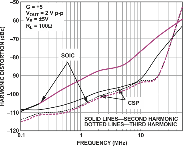
Another benefit is decreased second harmonic distortion. One cause of second-harmonic distortion in conventional op-amp pin configurations is the coupling between the noninverting input and the negative supply pin. The low-distortion pinout for the LFCSP package eliminates this coupling and greatly reduces second-harmonic distortion; in some cases the reduction can be as much as 14 dB. Figure 12 shows the difference in distortion performance between the AD8099 SOIC and the LFCSP package.
 |
||
| Figure 12. | AD8099 distortion comparison – the same op amp in SOIC and LFCSP packages. |
|
This package has yet another advantage – in power dissipation. The LFCSP provides an exposed paddle, which lowers the thermal resistance of the package and can improve θJA by approximately 40%. With its lower thermal resistance, the device runs cooler, which translates into higher reliability
Routing and Shielding
A wide variety of analog and digital signals, with high- and low voltages and currents, ranging from dc to GHz, exists on circuit boards. Keeping signals from interfering with one another can be difficult.
Recalling the advice to “Trust No One,” it is critical to think ahead and come up with a plan for how the signals will be processed on the board. It is important to note which signals are sensitive and to determine what steps must be taken to maintain their integrity. Ground planes provide a common reference point for electrical signals, and they can also be used for shielding. When signal isolation is required, the first step should be to provide physical distance between the signal traces.
Here are some good practices to observe:
- Minimizing long parallel runs and close proximity of signal traces on the same board will reduce inductive coupling.
- Minimizing long traces on adjacent layers will prevent capacitive coupling.
Signal traces requiring high isolation should be routed on separate layers and – if they cannot be totally distanced – should run orthogonally to one another with ground plane in between. Orthogonal routing will minimize capacitive coupling, and the ground will form an electrical shield. This technique is exploited in the formation of controlled-impedance lines.
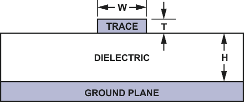
High-frequency (RF) signals are typically run on controlled-impedance lines. That is, the trace maintains a characteristic impedance, such as 50 ohms (typical in RF applications). Two common types of controlled-impedance lines, microstrip and stripline can both yield similar results, but with different implementations.
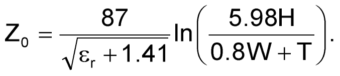
A microstrip controlled-impedance line, shown in Figure 13, can be run on either side of a board; it uses the ground plane immediately beneath it as a reference plane.
 |
||
| Figure 13. | A microstrip transmission line. | |
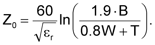
Equation 6 can be used to calculate the characteristic impedance for an FR4 board.
 |
(6) |
H is the distance in from the ground plane to the signal trace, W is the trace width, T is the trace thickness; all dimensions are in mils (inches × 10-3). εr is the dielectric constant of the PCB material.
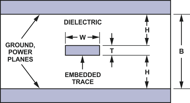
Stripline controlled-impedance lines (see Figure 14) use two layers of ground plane, with signal trace sandwiched between them. This approach uses more traces, requires more board layers, is sensitive to dielectric thickness variations, and costs more – so it is typically used only in demanding applications.
 |
||
| Figure 14. | Stripline controlled-impedance line. | |
The characteristic-impedance design equation for stripline is shown in equation 7.
 |
(7) |
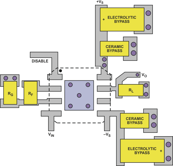
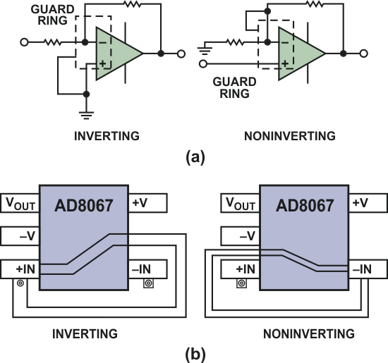
Guard rings, or “guarding,” is another common type of shielding used with op amps; it is used to prevent stray currents from entering sensitive nodes. The principle is straightforward – completely surround the sensitive node with a guard conductor that is kept at, or driven to (at low impedance) the same potential as the sensitive node, and thus sinks stray currents away from the sensitive node. Figure 15(a) shows the guard ring schematics for inverting and noninverting op-amp configurations. Figure 15(b) shows a typical implementation of both guard rings for a SOT-23-5 package.
 |
||
| Figure 15. | Guard rings. (a) Inverting and noninverting operation. (b) SOT-23-5 package. | |
There are many other options for shielding and routing. The reader is encouraged to review the references below for more information on this and other topics mentioned above.
Conclusion
Intelligent circuit-board layout is important to successful op-amp circuit design, especially for high-speed circuits. A good schematic is the foundation for a good layout; and close coordination between the circuit designer and the layout designer is essential, especially in regard to the location of parts and wiring. Topics to consider include power-supply bypassing, minimizing parasitics, use of ground planes, the effects of op-amp packaging, and methods of routing and shielding.
References
- Ardizzoni, John, “Keep High-Speed Circuit-Board Layout on Track,” EE Times, May 23, 2005.
- Brokaw, Paul, “An IC Amplifier User’s Guide to Decoupling, Grounding, and Making Things Go Right for a Change,” Analog Devices Application Note AN-202.
- Brokaw, Paul and Jeff Barrow, “Grounding for Low- and High-Frequency Circuits,” Analog Devices Application Note AN-345.
- Buxton, Joe, “Careful Design Tames High-Speed Op Amps,” Analog Devices Application Note AN-257.
- DiSanto, Greg, “Proper PC-Board Layout Improves Dynamic Range,” EDN, November 11, 2004.
- Grant, Doug and Scott Wurcer, “Avoiding Passive-Component Pitfalls,” Analog Devices Application Note AN-348.
- Johnson, Howard W., and Martin Graham, High-Speed Digital Design, a Handbook of Black Magic, Prentice Hall, 1993.
- Jung, Walt, ed., Op Amp Applications Handbook, Elsevier-Newnes, 2005.