TI Application Report
Introduction
For several years Quad-flat no-leads (QFN) package with thermal pad have been standard starting point for high current designs. Technology and trends pushed buck converters to get even smaller and more efficient. Therefore, optimized PCB designs need to be considered to dissipate the heat efficiently through the PCB and enable low operating temperatures.
Especially for thermally-limited designs, mitigating the heat effectively from the Integrated Circuit (IC) through the Printed Circuit Board (PCB) has become paramount. The PCB is the actual carrier and heatsink of ICs and therefore the influence of PCB on ICs thermal capability should be analyzed. This necessitates an optimal PCB layout design to ensure reliable operation of ICs over a wide range of temperature and different layouts can be realized depending on packaging technology and associated pinouts.
This application note discusses three different PCB design approaches and the cost trade-off for a high power density package. A brief comparison between simulated and measured results is subsequently explained. For the study, TI’s new TPS62866- 6 A buck converter in a 1.05-mm × 1.78-mm × 0.5-mm WCSP/DSBGA package, is considered. The package size is equal to die size in these packages for PCB space saving which makes heat dissipation from these packages more challenging.
Thermal Vias in Power PCB design
Usually, power PCB designs focus on improving thermal performances by increasing the copper area or adding ground planes in a multilayer boards. Thicker copper planes and wider traces resulting in low resistance and low parasitic inductance also helps to dissipate heat in the same size board area.
However, one of the most effective ways to propagate heat through the PCB is to use vias. Thermal vias are commonly used in PCBs as a mean to dissipate heat vertically from surface mount components to the PCB inner layers. Vias are simple mechanical drillings made to penetrate the PCB and thereby connect multiple layers in the PCB.
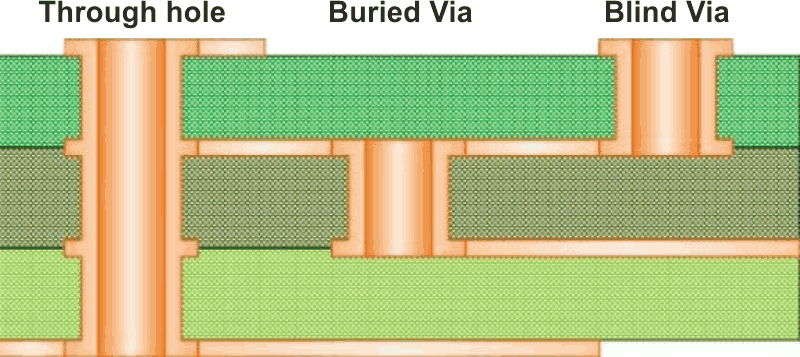
Figure 1 shows the different type of vias typically used in the PCB industry, they also differ in terms of use and costs.
 |
||
| Figure 1. | Different use of vias. | |
Through-hole vias are the most used and cheapest to manufacture. There are micro vias called buried vias: which can connect the internal layers without being exposed to outer air, and blind vias: which can connect the internal layers and are exposed on one side of the board. Both buried vias and blind vias provide only a partial connection between the PCB layers and add a degree of complexity to the design which results in a more expensive PCB design.
Layout Comparison of TPS62866
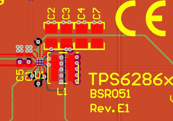
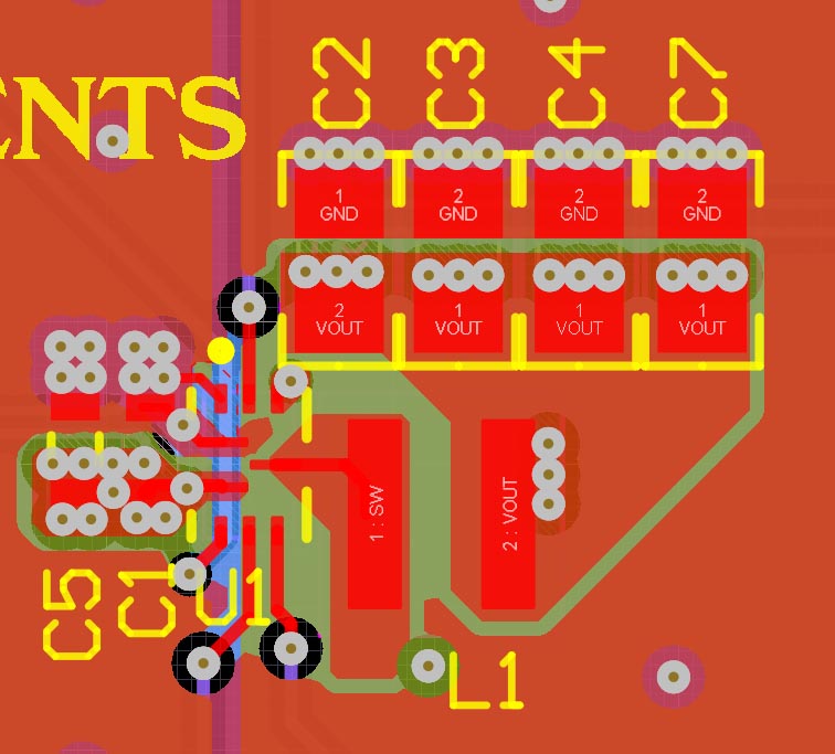
Three different versions of PCB are designed and studied for thermal analysis. In the E1 version (Figure 2), through-hole micro vias or thermal vias are placed under the device and near the VOUT net of the inductor. In the SW net of the device and the inductor, blind vias are provided. This is obviously a performance optimized solution.
 |
||
| Figure 2. | PCB Layout for E1. | |
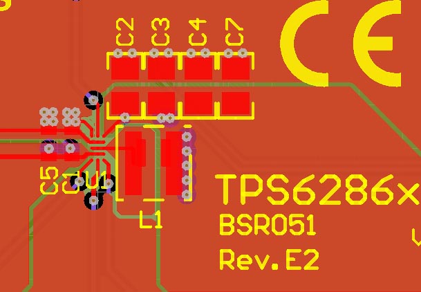
The E2 version (Figure 3) is a cost optimized solution and hence no vias are provided under the device as well as the inductor. But the micro vias near the VOUT net of the inductor is unchanged.
 |
||
| Figure 3. | PCB Layout for E2. | |
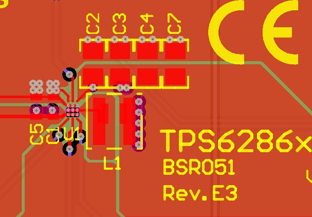
In the E3 version (Figure 4), a trade-off between cost and performance is achieved by providing through-hole micro vias under the device even in the SW net. Blind vias are not used under the device or the inductor. Micro vias near the VOUT net of the inductor is unchanged.
 |
||
| Figure 4. | PCB Layout for E3. | |
Simulation vs. Thermal Measurement
Simulation tools allow customer to evaluate their designs before manufacturing boards and assess the best implementation of their designs. Consequently, three versions of the PCB were simulated using Keysight’s Electro-thermal tool. The simulation setup considered is for VIN = 3.3 V and VOUT = 0.9 V at 6 A load and ambient temperature (typically 25 °C). The thermal images of the PCBs were then captured using FLIR T335 thermal imaging camera for the same test conditions. The results are as shown below.
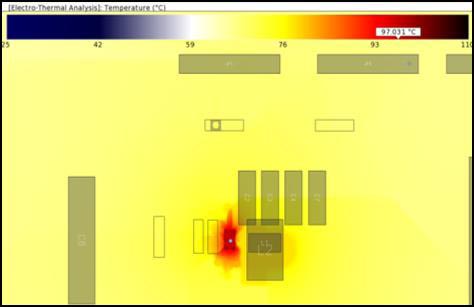
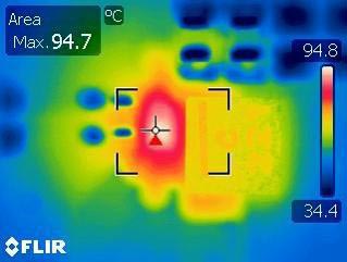
In the E1 version (Figure 5), the simulation and measurements resulted in a highest temperature of 97 °C and 94.7 °C respectively on the device.
|
||||
| Figure 5. | Simulation vs. Measurement for E1. | |||
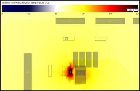
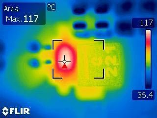
In the E2 version (Figure 6), the simulation and measurements resulted in a highest temperature of 107 °C and 117 °C respectively on the device.
|
||||
| Figure 6. | Simulation vs. Measurement for E2. | |||
In the E3 version (Figure 7), the simulation and measurements resulted in a highest temperature of 97.7 °C and 96 °C respectively on the device.
|
||||
| Figure 7. | Simulation vs. Measurement for E3. | |||
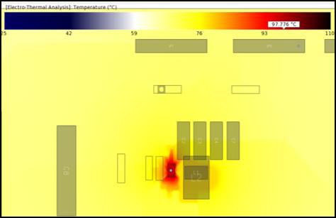
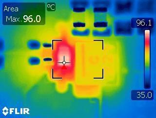
It is then clear that the simulation results are not exactly similar to measurement results and this solely depends on the assumptions of the simulation models and the inaccuracy of real-time measurements. Nevertheless, from both the simulation and measurement, the hottest point of the PCB is on the device. It is seen that the lowest temperature is for E1 version and the highest for E2 version. The temperature of the device in E1 and E3 versions are very much comparable.
In addition to the reduction of the thermal resistance of the device, the optimization of the layout for thermals also can offer improvements in terms of efficiency. The use of thermal vias allows a better connection of the switching plane to inner layers of the design, by providing a low resistive path and consequently increases the switch node copper area. The fast swinging from the input voltage to ground at high frequency makes the switch node a critical thermal connection.
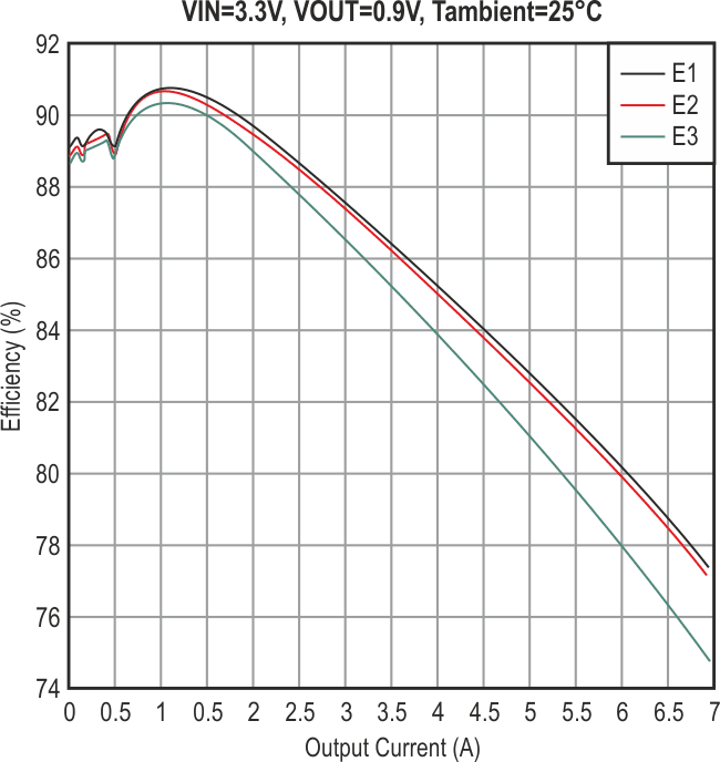
Table 1 shows the associated efficiency curves to the different layout implementations.
| Table 1. | PCB Layout Comparison Table | ||||||||||||||||
|
|||||||||||||||||
The efficiency curves comparison (Figure 8) reflects that better efficiency results can be achieved by increasing copper area at the switching node. Thus, it is important to consider wide connection at the switch node.
 |
||
| Figure 8. | Efficiency Comparison Between Layouts. | |
PCB Layout for Thermal Performance
In the E1 version, where both blind vias and through-hole thermal vias are used, best heat exchange is achieved between the package and the PCB. The device temperature is much lower in E1 compared to the other versions. Hence, it can be regarded as a performance optimized solution. On the contrary, blind vias are difficult to manufacture and this increases the overall cost of the PCB. In the E2 version, thermal vias are not used, heat is not dissipated effectively from the board and the device has very high temperature. But the overall cost is much lower than the other versions and hence it is a cost optimized solution.
In the E3 version, the device temperature is lower than the E2 version and almost similar to E1 version. This means, there is effective heat dissipation and the same thermal performance is achieved by using through-hole micro vias. Blind vias could be beneficial but in this case, it is not necessary. By avoiding unnecessary blind vias we can save cost and at the same time obtain a highly optimized design. Therefore, it is both performance and cost optimized.
Adding thermal vias helps reducing the overall device temperature and improves efficiency results. It is also manifest that after adding an optimum number of vias, using more thermal vias will not necessarily offer an additional reduction of the same magnitude.
 |
||
| Figure 9. | TPS62869EVM layout. | |
However, using vias directly on the switch node can propagate fast switching signals through the PCB and induce high switching noise which, in noise-sensitive applications, could disturb other signals on the board. For more noise-sensitive applications, the TPS62869EVM layout shows how to achieve good thermal results without using micro vias and thermal vias at the switch node (Figure 9).
Summary
Layout is essential to optimize the thermal performance of a high-density buck converter. Thermal vias play a significant role in vertical heat dissipation and they must be placed directly below or very close to the heating elements/components. Additionally, the effective thermal resistance of parallel vias in an array is much less than that for a single via. Hence a number of vias can be closely spaced for better heat dissipation.
If the component density is not too high on the PCB, through-hole micro vias would be sufficient to dissipate heat on the PCB. Blind vias are normally used in HDI PCBs where component density is too high and when multiple traces are present in the inner PCB layers which cannot be cut-through. Therefore, by using simple through-hole micro vias, we can achieve a performance and cost optimized solution.