Introduction
Flyback power converters are currently some of the most common converter topologies around. This is due to the simplicity of their design and the competitive size/cost/efficiency ratio their can deliver, especially in the mid-level power range (2 W to 100 W).
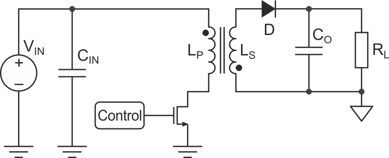
Like any converter topology, a flyback converter is composed of a power path and a control path. The power path is responsible for the converting power from one type to another, and is made up of the same elements as other switching power converters: two switches (a MOSFET and a diode), a capacitor, and an inductor. What sets the flyback converter apart from other converter topologies is the fact that the inductor is actually a pair of coupled inductors; in addition to storing power for the conversion process, these inductors add isolation between the primary side and the secondary side of the converter (see Figure 1).
 |
|
| Figure 1. | Circuit Schematic of a Flyback Converter. |
Although this article will be centered on the control path of the converter, it is convenient to include a short summary of the power path’s operation. A flyback converter has two operation phases, tON and tOFF, which are named after and controlled through the switching states of the MOSFET.
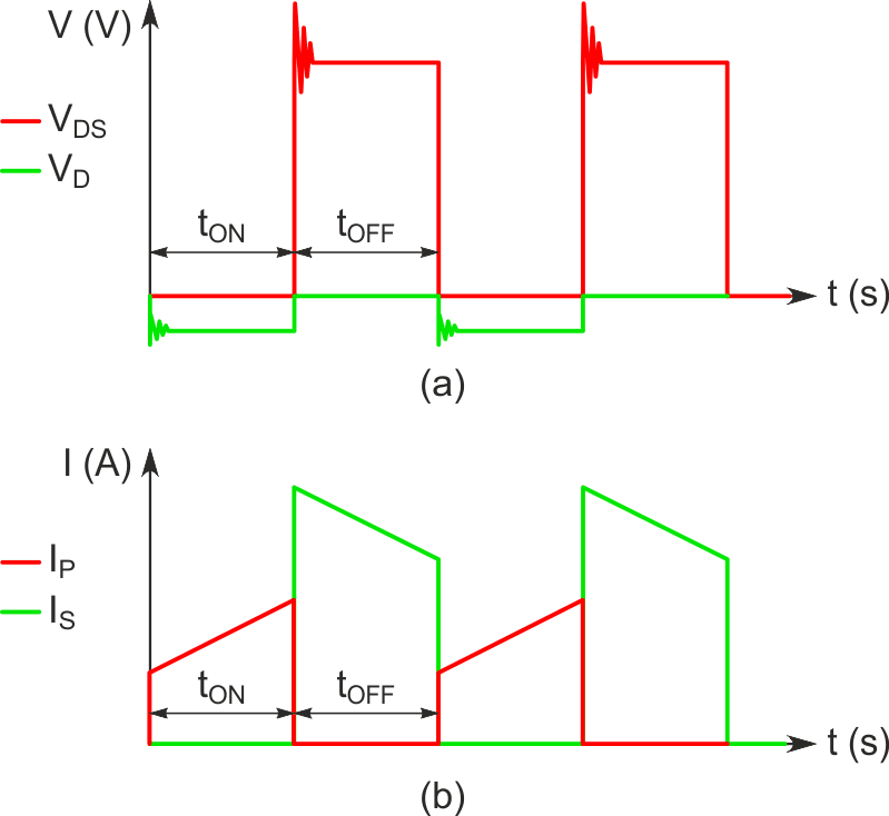
During tON, the MOSFET is on and current flows from the input through the primary inductor, linearly charging the coupled inductor and creating a magnetic field around it (see Figure 2.b). In the secondary inductor, the rectifier diode is reverse-biased, which means the transformer is disconnected from the output (see Figure 2.a).
 |
|
| Figure 2. | a) Voltage in MOSFET and Diode b) Current in Primary and Secondary Coils. |
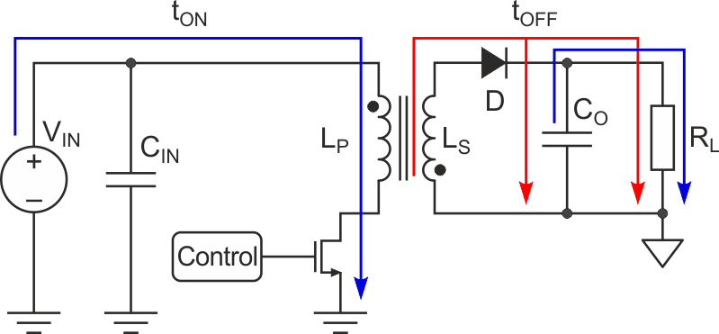
The charge stored in the output capacitor is responsible for maintaining a stable voltage at the load (see Figure 3).
 |
|
| Figure 3. | Current Diagram of a Flyback Converter. |
During tOFF, the MOSFET is open and the coupled inductor begins to demagnetize through the diode, which is now directly polarized. The current from the inductor then charges the output capacitor and powers the load.
Although the power path is responsible for the conversion process, there is a second element to consider in converter design: the control loop. This control path is necessary due to the presence of perturbations in the system, such as fluctuations in the power source or changes in the load. The goal of the control system is to ensure stable operation, regardless of perturbations in the system.
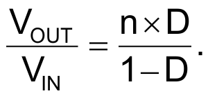
As with most switching converters, the flyback’s output voltage is controlled through the MOSFET’s duty cycle. This can be easily understood by observing the flyback controller’s transfer function using Equation (1):
 |
(1) |
Equation (1) shows that as the value of D (duty cycle) increases, the converter’s gain also increases, thus increasing the output voltage. Therefore, the controller modifies the signals it sends to the MOSFET’s gate to compensate for any changes it senses in the converter’s output.
The converter must first sense these changes in the output voltage, treat this voltage correctly, and then regulate the transistor’s gate voltage accordingly. For more accurate control, many control paths include a current control loop, which helps improve regulation and power factor by sensing the current flowing through the primary inductor. This is the case for the most commonly used flyback converter control technique: peak current control mode (see Figure 4).
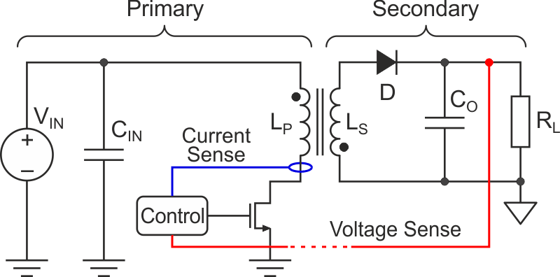 |
|
| Figure 4. | Peak Current Control Mode Schematic. |
Primary-Side and Secondary-Side Regulation
The main problem that arises with flyback converters is the preservation of isolation. As mentioned previously, one of the main advantages of flyback converters is that they include magnetic isolation between the input and the output. This divides the circuit into two halves, called the primary side and secondary side. Isolation is crucial for protecting any devices connected to the output from possible current leaks that could break the devices down, or even cause harm to end users.
Consequently, isolation must be maintained, which means that there must be no conduction path connecting the primary and the secondary sides of the circuit. This is not absolute, however; voltage source transformers are normally allowed a maximum leakage of 10 mA and require isolation of at least 3 kV. But leakage between the primary and secondary sides must still be minimized as much as possible.
This also includes the controller, which means that designers must find a way of sensing the output voltage of the converter without bypassing the isolation barrier. Two regulation methods can be implemented: primary-side regulation and secondary-side regulation.
Primary-Side Regulation
In a real application, the controller IC requires an auxiliary output from the transformer to supply the IC circuitry (see Figure 5). Due to transformer characteristics, this auxiliary transformer output is directly related to the converter’s output voltage. Therefore, by knowing the transformer’s turn ratio, this output can be used to regulate the system. This is called primary-side regulation (PSR), and this method enables a rough regulation of the output using very few components. Most PSR control ICs also include compensation circuits, which significantly reduce design time.
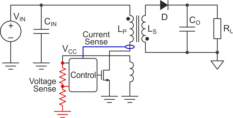 |
|
| Figure 5. | Primary-Side Regulation Circuit Schematic. |
Another benefit of primary-side regulation is that it minimizes the number of paths that cross the isolation barrier. This is especially useful in high-voltage applications, because it reduces the isolation voltage requirements of the components, which also has lowers total cost.
However, primary-side regulation has some drawbacks. For example, the sampling of the reflected output voltage on the auxiliary winding occurs only once every PWM cycle. PSR regulation systems often implement knee-point sampling, which is a method that samples the voltage at the time when inductor current is at its lowest value. This significantly reduces ringing in the circuit, but also means that in between switching cycles there is no monitoring of the voltage value. Therefore, transient regulation is slower than in secondary-side systems, where the output voltage is constantly monitored.
In addition, regulation has poorer performance when multiple outputs are implemented, especially if the loads attached to each winding vary significantly. This occurs because the heaviest load is typically chosen to implement the feedback, so it alone determines the control loop’s response.
Secondary-Side Regulation
If more accurate regulation is necessary, secondary-side regulation (SSR) can be implemented (see Figure 6). This method directly senses the output voltage and sends the signal to the converter through an optocoupler, so as to transmit the signal without breaking the isolation barrier between the primary and secondary sides. Secondary-side regulation is much more accurate, even when there are one or more outputs at the secondary side. This is mainly because cross-regulation between various secondary windings is much better than it is between the primary and secondary windings. Secondary-side regulation also allows for the implementation of different techniques to optimize regulation performance, such as the use of escalated windings in the transformer or weighted feedback techniques.
However, secondary-side regulation comes with its own set of drawbacks. For instance, SSR control loops require more components, especially if the voltage is compensated at the secondary side before being sent to the controller placed on the converter’s primary side. This increases the converter’s size and cost, while simultaneously reducing reliability due to the optocoupler’s degradation over time.
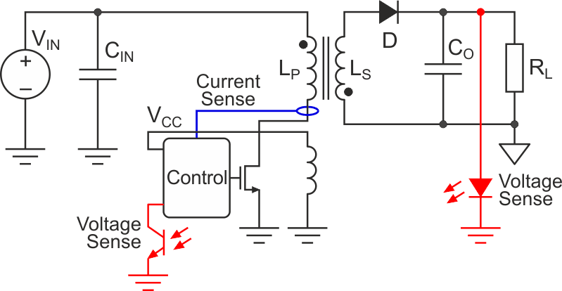 |
|
| Figure 6. | Secondary-Side Regulation Circuit Schematic. |
Summary
There are two differentiated methods for implementing a control loop in your converter design: called primary-side regulation and secondary-side regulation (PSR and SSR, respectively). Each method has its own set of advantages and disadvantages, which have been discussed in the sections above and are summarized below (see Table 1).
| Table 1. | The main features of methods for the output voltage stabilizing of flyback converters | ||||||||||||||||||||||||
|
|||||||||||||||||||||||||