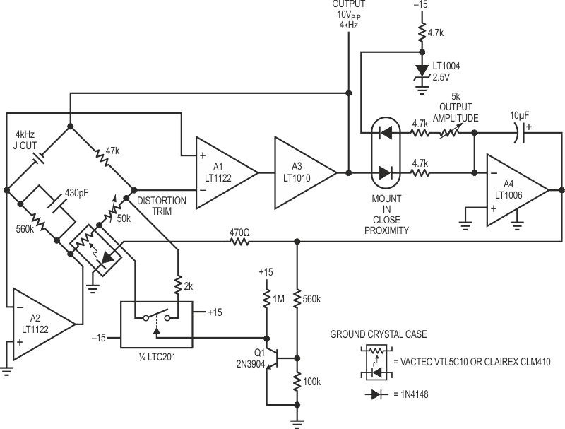
A spectrally pure sine wave oscillator is required for data converter; filter and audio testing. Figure 1 provides a stable frequency output with extremely low distortion. This quartz stabilized 4 kHz oscillator has less than 9 ppm (0.0009%) distortion in its 10 VP.P output.
 |
|
| Figure 1. | Quartz stabilized 4 kHz oscillator with 9 ppm distortion. |
To understand circuit operation, temporarily assume A2’s output is grounded. With the crystal removed, A1 and the A3 power buffer form a noninverting amplifier with a grounded input. The gain is set by the ratio of the 47k resistor to the 50k potentiometer – opto-isolator pair. Inserting the crystal closes a positive feedback path at the crystal’s resonant frequency, and oscillations occur. A4 compares A3’s positive peaks with the LT1004 2.5 V negative reference. The diode in series with the LT1004 provides temperature compensation for A3’s rectifier diode. A4 biases the LED portion of the opto-isolator, controlling the photo resistor’s resistance. This sets loop gain to a value permitting stable amplitude oscillations. The 10 µF capacitor stabilizes this amplitude control loop.
A2’s function is to eliminate the common mode swing seen by A1. This dramatically reduces distortion due to A1’s common mode rejection limitations. A2 does this by servo controlling the 560 kΩ-photocell junction to maintain its negative input at 0 V. This action eliminates common mode swing at A1, leaving only the desired differential signal.
Q1 and the LTC201 switch form a start-up loop. When power is first applied oscillations may build very slowly. Under these conditions A4’s output saturates positive, turning on Q1. The LTC201 switch turns on, shunting the 2 kΩ resistor across the 50 kΩ potentiometer This raises A1’s loop gain, forcing a rapid build-up of oscillations. When oscillations rise high enough A4 comes out of saturation, Q1 and the switch go off and the loop functions normally.
The circuit is adjusted for minimum distortion by adjusting the 50 kΩ potentiometer while monitoring A3’s output with a distortion analyzer. This trim sets the voltage across the photocell to the optimum value for lowest distortion. The circuit’s power supply should be well regulated and bypassed to ensure the distortion figures quoted.
 |
|
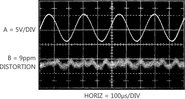
| Figure 2. | Oscillator output and its 9 ppm distortion residue. |
After trimming, A3’s output (trace A, Figure 2) contains less than 9 ppm (0.0009%) distortion. Residual distortion components (trace B) include noise and second harmonic residue. Oscillation frequency, set by crystal tolerance, is typically within 50 ppm with less than 2.5 ppm/°C drift.