Despite the increasing availability and declining cost of on-chip analog peripherals, the humble PWM DAC retains its appeal as a “free” DAC [1] that can repurpose an uncommitted DIO pin and counter/timer module, add a simple low pass ripple filter, and become an (albeit imperfect but still useful) analog output.
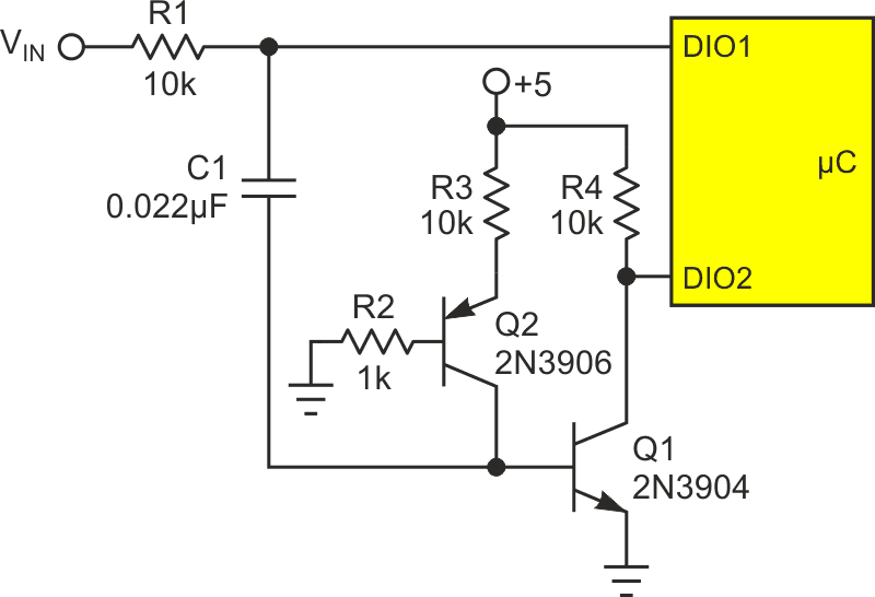
Okay, but what about the other end of the analog/digital/analog signal chain? How close can we come to a (albeit imperfect but still useful) zero cost ADC? Figure 1, with its two transistors, four resistors, and one capacitor is my “free” (< $0.50 in singles) ADC.
 |
|
| Figure 1. | Circuit of a “free” (approximately) ADC. |
Here’s how it works.
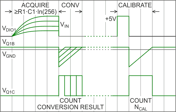
Tri-stateable I/O pin DIO1, when programmed for high impedance, allows the top end of C1 to charge through R1 and acquire input voltage VIN, as shown in the ACQUIRE phase of Figure 2.
 |
|
| Figure 2. | Acquire, convert, and calibrate phases of “free” ADC. |
The minimum duration of the DIO1 = high-Z acquisition phase is determined by N (the desired number of bits of conversion precision) and the R1C1 time-constant.
Minimum acquisition interval = R1C1×ln(2N).
For example, for the RC values shown and N = 8, the minimum interval = ~1.5 ms. If N = 12, the minimum interval would be ~2 ms. While C1 is charging, Q1’s forward-biased and saturated base provides a low impedance (~1 Ω) path to ground with an offset (VQ1B) of ~650 mV. The acquisition phase ends with DIO1 being reprogrammed for a 0 output. This drives the top end of C1 to ground, and VQ1B negative, turning Q1 off. Q1 turning off allows DIO2 = 1, which is intended to be programmed so to enable a microcontroller counter/timer peripheral to begin counting clock cycles (e.g., 1 MHz) and thus measure the duration of Q1 = OFF.
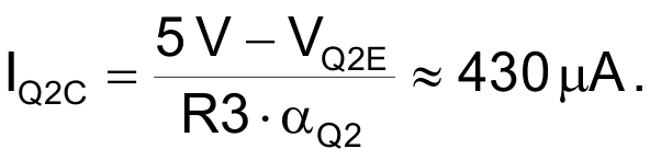
Q1 = OFF (and therefore counting) continue until C1’s negative charge dissipates and allows VQ1B to return to the 650 mV. The time that elapses (and therefore cycles counted) while this happens is directly proportional to VIN and inversely proportional to current source Q2’s collector current.
C1 recharge interval = C1×VIN/ IQ2C
So that…
counting interval = 51 µs/V and conversion count = 51×FCLK(MHz)×VIN,
approximately!
R2 is provided to avoid Q2 saturation. R4 is Q1’s collector and DIO2’s pullup. Combining acquisition (1.5 ms) and conversion (256 µs for 8 bits with 1 MHz clock) times predicts a max conversion rate of ~560 samples/sec. Okay so far.
But how to cope with that “approximately” thing? It covers a multitude of “free” circuitry limitations, including tempco’s of inexpensive resistors, capacitors, and transistor bias voltages and current gains so simply ignoring it simply won’t do.
Fortunately, as suggested by the right side of Figure 2, this “free” ADC incorporates a self-calibration feature.
To self calibrate, DIO1 is programmed for output, set to 1 to charge C1, then to 0 to generate a counting interval and NCAL count value. Subsequent conversion results are then scaled as…
VIN = 5V×conversion_count/NCAL
…which corrects for most of the error sources listed above. But unfortunately, not quite all.
One that remains is an uncorrected zero offset due to the minimum VQ1B excursion needed to turn Q1 off and generate a non-zero counting interval. The least VIN required to do so is approximately
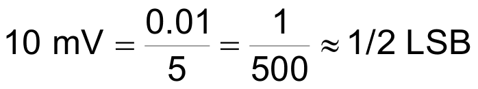
of an 8 bit conversion result of full-scale 5 V.
Which leaves just one obvious source of potential inaccuracy: the 5 V supply. Logic supplies are not the best choice for an analog reference and the accuracy of this “free” ADC will ultimately depend on how good the one used actually turns out to be.
Of course, the classic PWM DAC suffers from exactly the same logic-supply-limitation malady, but this hasn’t negated its utility or popularity.
Which sort of takes the topic of “free” analog peripherals back to where it began. Albeit imperfect – but still useful?