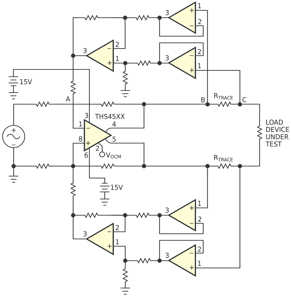
Many precision test-and-measurement and high-speed analog applications require an exact targeted voltage to be delivered to the device under test or intended load to accurately analyze the device. Design and test engineers are well-aware that this goal is sometimes unattainable, because the impedance across the traces delivering the signal to the load alters the original signal. Traditionally, engineers use a Kelvin connection to measure the accurate voltage that the load or the device under test sees at its terminals. The Kelvin-connection method enables you to accurately measure the voltage at the load terminal, but it may not correct for the voltage drop or the phase shift that occurs dynamically across the signal lines with various impedances. In high-frequency signals, the RLC (transmission-line effects) of the traces come into play and cause a significant signal phase shift. As a result, designers always look for the least expensive methods to correct the voltage drop and the phase shift across the transmission lines. The circuit in Figure 1 is a fully differential line driver comprising a fully differential amplifier and two high-frequency, high-impedance feedback paths.
 |
|
| Figure 1. | This fully differential circuit compensates for voltage drop and phase shift in transmission lines. |
The resistance associated with each trace causes a voltage drop through the path. Thus, the signal amplitude delivered to the load is lower than the signal amplitude at the output of the fully differential line driver. This voltage drop is proportional to the resistance value of the trace, RTRACE, and the current flow through the corresponding trace. For example, if the output current of the line driver is 100 mA and the trace resistance is 10 Ω, a 1 V drop develops across RTRACE. As a result, if the output amplitude is 10 V p-p, the load sees a 9 V p-p signal. The feedback paths, which work as subtracters, accurately measure this voltage drop. The feedback paths measure the voltage drop across RTRACE. This voltage then adds to the input of the line driver at the summing Node A. Because the circuit is symmetrical, the same function occurs at the opposite corresponding points. As a result, regardless of the value of the total voltage drop across RTRACE, the subtracter measures it and adds it back into the input signal of the line driver. Consequently, the output of the line driver increases by the measure of the voltage drop across RTRACE, and the load sees the exact voltage it was initially intended to see. Because the circuit is a closed-loop system and has negative feedback, the circuit remains in a stable condition.
The buffers in the feedback paths form a high-input-impedance node to prevent any load alteration. For example, without buffers, the series and parallel resistors of the subtracter would cause the value of the load to vary. These buffers, in conjunction with the subtracter, form an instrumentation amplifier. You can adjust this configuration for different gains to create variations of this circuit for different applications. The instrumentation amplifier creates a high-input-impedance path that works similarly to the sense lines of a Kelvin connection. The main difference is that the sense line in this circuit measures the actual voltage drop across RTRACE over various frequencies and adds it back to the original signal. You should pay attention to the ratio of the line driver's gain configuration and the subtracter's gain configuration to ensure stability of the circuit. Additionally, you should verify that the bandwidths of the feedback-path devices are greater than the bandwidth of the line driver to prevent any added errors to the system via feedback paths' bandwidth limitations. You may choose to design the feedback paths with much greater bandwidth than the line driver (two times greater, for example). Doing so enables this circuit to correct the phase shift across the transmission line if the traces manifest RCL characteristics.
 |
|
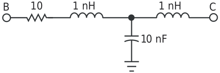
| Figure 2. | This circuit represents a simulated transmission line inserted between points A and B of the circuit in Figure 1. |
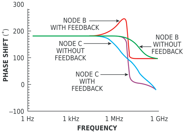
For example, assume that you insert a transmission-line model between nodes B and C in the circuit of Figure 1, as in Figure 2. The bandwidth of the fully differential amplifier is 300 MHz at unity gain, and the input signal is 2 V p-p. The bandwidth of the feedback paths is 600 MHz to prevent any added phase shift to the signal from the feedback circuit. Configuring the test circuit as such lets you see the phase shift that the transmission line alone introduces. The transmission line causes a significant phase shift in the signal delivered to the load. Figure 3 shows the phase-shift curves at Node B before the transmission line and at Node C after the transmission line, right above the load. These curves show the effect of the feedback path in correcting the phase shift at the end of the transmission line where the load is located. This circuit configuration essentially corrects the phase shift of the signal that the RCL of the transmission line causes. The fully differential line driver enables you to deliver twice the voltage swing across the load as opposed to using a single-ended line driver with the same power supplies and similar specifications. However, the nature of fully differential configurations requires that you pay close attention to maintaining the balance of passive and active components to preserve the signal integrity delivered to the load. Therefore, you should set equal resistor values on the top and the bottom feedback paths. This design can correct for voltage drop and phase shifts across the transmission lines in low- and high-frequency cases. Design simplicity and the fact that the design uses few components make it cost-effective for many applications dealing with voltage-correction and phase-shift issues.
 |
|
| Figure 3. | The phase-shift curves at Node B before the transmission line and at Node C after the transmission line show the effect of the feedback path in correcting the phase shift at the end of the transmission line. |