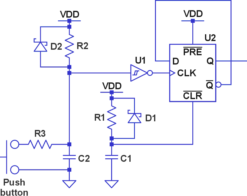
Applications for using a single pushbutton to advance a circuit to its next logical state are legion. Typically, there are just “on” and “off” states, but there can be more. The heart of the circuit is a toggle flip-flop (or, for more states, a counter or shift register) which responds to a clock transition.
The successful circuit prevents the contact bounce of the mechanical pushbutton from generating more than one “clock” for every push and release of the button. It’s also desirable for the circuit to initialize upon power-up to a specific state and for the press of the pushbutton (from a human point of view) to immediately cause a state change. The basic circuit of Figure 1 has these features.
 |
|
| Figure 1. | U1 is a Schmitt inverter and U2 a D-type flip-flop. The diodes are small-signal Schottky types. The pushbutton is normally open. See the text for a discussion of resistor and capacitor values. |
Upon loss and discharge of the VDD supply, the Schottky diodes discharge C1 and C2 to nearly zero volts. Time constant R1C1 should be at least 10 times larger than the supply turn-on time so that the power-up sequence starts and ends with U2’s Q being cleared.
Also, upon power up, U1’s output starts out as a logic high and transitions low after R2 charges C2. Since U2’s active clocking transition is low to high, this leaves Q initialized low. The R2C2 time constant should be on the order of 1 second.
R3 is optional and limits initial C2 discharge currents when the normally open pushbutton is pressed. If R3 is used, it should be chosen so that momentary contact bounce closures nearly completely discharge C2 in 10 ms or less.
C2 and R2, along with the Schottky inverter U1, work to prevent contact bounce from producing extra transitions, which would otherwise toggle flip-flop U2. After the pushbutton is released and R2 is starting to charge C2, additional button pushes will not toggle U2. This is because the output of U1 is still high and so cannot transition from low-to-high to toggle U2. This is an argument against making the R2C2 time constant too large.
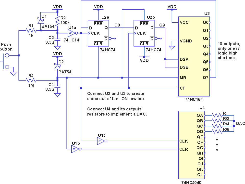
Figure 2 shows how the circuit of Figure 1 can be extended into a multi-state 10-position switch with only one active high output at a time, or into a digital-to-analog converter (DAC).
 |
|
| Figure 2. | A 10-position switch with only one active high output at a time, and a DAC are shown. |
If fewer than 10 states are desired for the switch, the U2a “D” input can be connected to a different U3 output. For the DAC, resolution can be extended to 12 bits with 12 resistors. Monotonicity will be somewhat less than that, and even with 0.1% resistors, accuracy will be even less than that. To avoid excessive loading of the outputs, no resistor should be less than 10 kΩ.