PN-junction diodes often have a dropout voltage of approximately 1.2V for silicon power diodes. That voltage drop causes power diodes to dissipate considerable power, resulting in a loss of efficiency in a power supply. In a photovoltaic panel with 120W of power and 24V nominal voltage, an antireturn diode may cause a power loss of 6W, or 5% of the managed energy. Moreover, the cost of developing a cooling system for dissipating the heat diodes may pose a problem.
This Design Idea shows a more efficient approach that replaces a conventional power diode with a MOSFET transistor operating in on/off mode.
 |
|
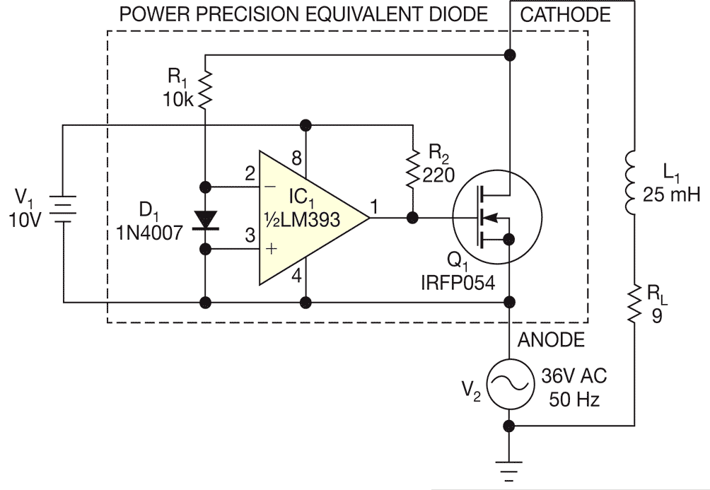
| Figure 1. | The precision power diode works as a rectifier that supplies power to an inductive load. |
Figure 1 shows the rectifier circuit with a MOSFET transistor, Q1, which has a low drain-to-source resistance in the on state. In the circuit, V2 represents an ac power source of 36V. The load comprises 9Ω resistor RL and 25-mH coil L1. Comparator IC1 generates the gate voltage for Q1 when the voltage-supply anode is higher than the drain-voltage cathode. Thus, the source works as the anode of the rectifier, and the drain functions as a cathode. The circuit exploits the capability of the transistor in conducting currents in the source-to-drain direction. Turning on Q1 effectively shorts its parasitic diode between the substrate and the drain, minimizing power loss. When the gate-to-source voltage is low, both Q1 and its parasitic diode are off. Diode D1 and resistor R1 limit the voltage across the comparator inputs.
 |
|
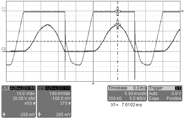
| Figure 2. | These traces show the rectifier’s waveforms for an inductive load that comprises 9Ω resistor RL and 25-mH coil L1. Trace C2 shows a maximum load current of 2.65A. (The probe is 100 mV/A.) Trace C1 shows the anode-to-cathode voltage drop. |
Figure 2 shows the load voltage and the voltage drop on rectifier Q1.
 |
|
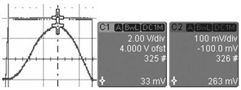
| Figure 3. | These traces show the condition of the rectifier with gate control. The MOSFET’s parasitic diode is off, and the maximum voltage drop across the MOSFET is only 33 mV (Trace C1). Trace C2 shows the current through the rectifier. |
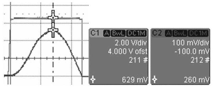
Figure 3 shows the normal operation of the rectifier, in which, for a maximum load current of 2.65A, the voltage drop is 33 mV; Q1 is working in the ohmic region. On the contrary, if you use the MOSFET, the voltage drop becomes 629 mV, yielding a maximum instantaneous power of 1.66W (Figure 4).
 |
|
| Figure 4. | These traces show the condition of the rectifier without gate control. The MOSFET’s parasitic diode is on, and the voltage drop across the MOSFET is 629 mV (Trace C1). Trace C2 shows the current through the rectifier. |
This approach is valid for any type of rectifier with any number of diodes. Moreover, you can use this circuit in dc/ dc and dc/ac converters because, when you use power MOSFETs in bridge circuits, they can conduct both active and reactive currents. This approach avoids the need to use substrate-drain parasitic diodes in the MOSFET.