The circuits presented here use an analog switch – such as a DG419 or one-third of a CD4053 – to combine an analog signal with a standard PWM signal. Most microcontrollers can easily generate the PWM signal. Combining the PWM signal with the analog signal and low-passing the result effectively multiplies the analog signal by a digital value. Such a circuit can be useful in signal processing, power factor correction, automatic gain control, and sensor interfacing. All four circuit variants rely on the same principle: using the analog switch to adjust the duty-cycle ratio between two analog input levels, and a lowpass filter (LPF) to eliminate the PWM chopping frequency.
 |
|
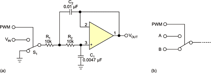
| Figure 1. | The use of an analog (CMOS) SPDT switch and an op amp configured as an LPF forms a simple multiplier circuit that can be used as either a digitally controlled gain block (a) or a cross-fader (b). |
Figure 1a depicts a multiplier incorporating a second-order Sallen-Key LPF. The active filter provides the best ac performance, effectively eliminating the chop frequency and passing slower ac signals through with minimal attenuation. Since the analog switch is selecting either the analog input signal or ground, the output voltage is equal to
VIN × D,
where
D is the duty cycle of the PWM signal; its value ranges from 0 to 1.
Figure 1b shows a variation of this circuit. Using the switch node formerly grounded as an additional analog input produces a circuit that gives an output equal to
(A×D) + B×(1 – D).
The PWM duty cycle selects the ratio between the two input signals and presents the result at VOUT.
The filter cutoff frequency should be optimized for the PWM frequency used. The values depicted provide a ∼10-kHz cutoff frequency. This should be satisfactory in most applications for an 8-bit PWM clocked at 16 MHz (a PWM frequency of 62.5 kHz). Response time will be less than 200μsec; noise will be less than 1 LSB. The cutoff frequency can be easily changed by adjusting R1 and R2, or C1 and C2. It is important that R1 = R2 and C2 ≈ 0.5 × C1. Doubling the resistor or capacitor values will halve the cutoff frequency; halving them will double the frequency.
 |
|
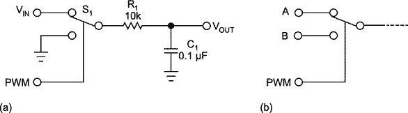
| Figure 2. | The active two-pole LPF can be replaced with a simpler single-pole passive circuit when slower response times are acceptable. Again, depicted are a gain block (a) and a cross-fader (b). |
Figures 2a and 2b show a simpler version of the previous circuits; they have a much slower response, however, and hence are useful only for generating a dc voltage or a low-frequency ac signal. Again, the roll-off of the LPF should be optimized to block the PWM frequency. For the 8-bit PWM frequency described earlier, the depicted 10k and 0.1 μF provide a response time of 5-msec and less than 1 LSB of noise.
Since all of the circuit variations have a dc gain of 1, the discrete component values affect ac performance only. These circuits are capable of high dc precision without the use of expensive precision components.