Application Note AND9151/D
November 2013
Creating and distributing clock signals are the heartbeat of digital systems. Today's high-end systems demand extremely low noise clock signal integrity. Jitter, and more recently, phase noise, are the most significant parameters when considering clock distribution timing budgets. Jitter is a time domain parameter while phase noise is its frequency domain equivalent.
There are several technical jitter definitions and terms to introduce before we understand Additive Phase.
- Jitter. Jitter - Jitter is the short-term frequency instability and is normally seen in the time domain on an oscilloscope.
- Phase Noise - Phase Noise is a ratio of signal power to noise power normalized to a 1 Hz bandwidth at a given offset from the carrier signal and is measured in the frequency domain on a phase noise analyzer. It is typically expressed as Single Side Band (SSB).
- Phase Jitter - Phase Jitter measures the amount of energy present in the specified frequency offsets from the carrier signal compared to the energy of the carrier signal by integrating the area under the phase noise plot.
- Noise Floor - Noise Floor is the noise level below which signals cannot be detected under the same measurement conditions. If an ideal clock is connected to the input of a buffer, the output phase noise of the buffer device is subtracted by the phase noise of the input clock signal. The generated phase noise of the buffer is also its noise floor. Noise floor is considered to be the lowest point of the plot. A buffer's Noise Floor can also be calculated from its phase noise measurement when a clean signal generator is the input source; see below.
- Additive Phase Jitter - Additive Phase Jitter is the amount of jitter caused by the device and is added to the input signal's phase jitter. In other words, it is the jitter contributed by the device. As will be demonstrated in this report, this value is highly dependent on the phase jitter of the input source. (Important Concept!) To reiterate, Additive Phase Jitter of the device is an addition to the input signal noise, and is integrated under the Single Side Band (SSB). As an example, SONET uses a frequency offset of 12 kHz to 20 MHz from the carrier signal to integrate the area under the phase noise plot to measure phase jitter.
The NB3V8312C is an ON Semiconductor high performance, low skew LVCMOS fanout buffer which can distribute 12 ultra-low jitter clocks from an LVCMOS/LVTTL input up to 250 MHz.
Download Application Note AND9151/D (557 Kb)
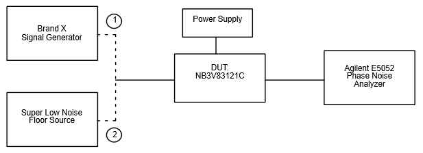
Basic Lab Setup for Phase Noise and Additive Phase Jitter