Simple DACs realized by lowpass filtering microcontroller-generated pulse-width-modulated (PWM) signals have a response that is typically a tenth of the PWM frequency. This Design Idea is a novel implementation of a previously published method [1] employing a reference ramp whose output is sampled and held by the PWM signal. This approach results in a throughput rate equal to the PWM frequency.
 |
|
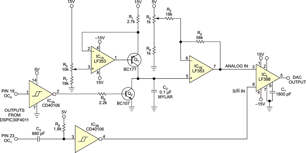
| Figure 1. | The off-page microcontroller generates signals for ramp control (OC4) and sample timing (OC1). |
You can use the circuit in Figure 1 to implement a ±10V 10-bit DAC with a throughput of 20 kHz. A dsPIC30F4011 microcontroller (not shown) is operated at a clock frequency of 96 MHz to generate the capture signals OC1 and OC4. Clock/4 is fed to an internal 16-bit timer whose period is set for a count of 1200 corresponding to a PWM frequency of 20 kHz. Signal OC4 is mostly high and goes low at a fixed count of 1170 as a reference for ramp generation. IC1A, along with Q1, forms a precision constant-current source that linearly charges capacitor C2 when Q2 is off. This signal inverted by IC3A switches Q2 on for a period of 30 counts to discharge C2 for the start of the next ramp. IC1B buffers, amplifies, and offsets the ramp; potentiometers R2 and R5 adjust the offset and gain.
The OC1 falling edge controls the PWM DAC sample timing relative to the ramp voltage. The data word to be converted determines the OC1 duty cycle by comparing it internally in the microcontroller with the internal 16-bit timer. C3 and R9 differentiate the resulting PWM signal; IC3B then inverts it, forming a 1-µsec sample signal for the sample-and-hold IC2. Pin 5 of IC2 forms the DAC output and is adjusted to −10, 0, and +10V for OC1 PWM counts of 88, 600, and 1112, respectively, corresponding to a 10-bit count of 1024.
The count offset of 88 helps to avoid the initial nonlinear region of the ramp so that the PWM DAC shows good linearity with a LSB of 20 mV and an accuracy of ±40 mV. Additional PWM DACs could also be implemented using capture PWM outputs OC2 and OC3.
 |
|
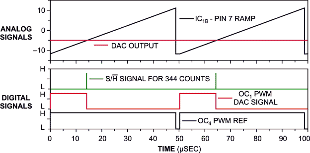
| Figure 2. | The differentiated OC1 falling edge generates the S/H sample pulse at the ramp − 5V point. |
Figure 2 shows the waveforms to be expected for a DAC output corresponding to 256 on a 10-bit scale of 1024. OC4 forms the PWM reference based on which a 20-kHz bipolar ramp signal is output at Pin 7 of IC1B. This ramp is sampled and held at a count of 256 + 88 = 344, corresponding to a DAC output of −5V.
References