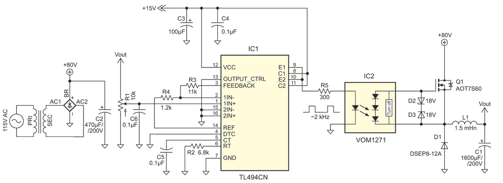
Power supplies with adjustable DC output ranging from 0 V to 30 V or 60 V are on the market. Above 60 V, there are not many. This Design Idea offers a solution.
There are many fixed voltage switching mode power supplies (SMPS) available, and connecting several in series can give us a higher fixed voltage. To obtain an adjustable output either from a SMPS or conventional transformer based supply, one needs to use a linear regulator or a switched mode buck converter. For a buck converter, a MOSFET or an IGBT can be used as a switching element.
Usually, for a high side switch, an IC with bootsrap operation or a pulse transformer is used. There are few photovoltaic couplers available to drive MOSFETs. As they do not provide much current to charge the gate capacitance quickly, these photovoltaic couplers are mainly used to drive low frequency MOSFET switches, such as solid state relays.
Here (Figure 1), an attempt has been made to use a photovoltaic coupler (VOM1271) in a switching regulator. This coupler has a built-in fast turn-off device. With a gate capacitance of 200 pF connected to IC2, switching times tON and tOFF are 53 µs and 24 µs, respectively. Considering this, a switching frequency of 2 kHz was chosen for the buck converter. A Texas Instruments TL494 (IC1) was chosen as a pulse-width-modulation controller.
 |
|
| Figure 1. | HV buck converter schematic. |
An AOT7S60 MOSFET was chosen as a switching element, considering gate threshold voltage (VGS(th)), total gate charge (QG), drain-source voltage (VDS), and drain current (ID). As the VOM1271 can provide about 8.4 V, VGS(th) should be well below this value; Q1’s VGS(th) is 3.9 V, and at 8.4 V it is well into conduction. IC2 cannot deliver much current (typically 45 µA). To ensure switching speed and reduce switching loss, gate charge should be low. The MOSFET has QG of 8.2 nC.
The buck converter was tested with a step down line transformer output after being rectified and filtered as shown in Figure 1. The output voltage is continuously adjustable from 5 V to 70 V by varying R1.
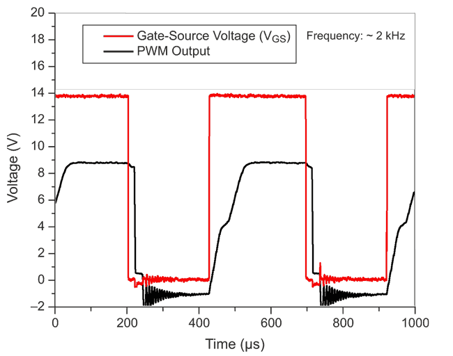
Figure 2 shows the gate-source voltage waveform and the IC1 output waveform at 70 V output and 230 Ω load.
 |
|
| Figure 2. | The gate-source voltage waveform and the IC1 output waveform at 70 V output and 230 Ω load. |
It is seen that though tOFF is fast enough, tON is about 80 µs. This is considered to be a slow turn-on for many switching applications. However, for a switching frequency of 2 kHz, it should not cause much switching loss, especially for a load condition when the PWM duty cycle is large.
Though L1 has a smaller value than calculated for the range of output voltage, the ripple was 80 – 120 mVP-P for loads ranging from 80 Ω – 230 Ω. Ripple was 80 mVP-P at 70 V output and 230 Ω load. Line regulation was 0.75% at the same operating condition. Though the efficiency varies with the operating condition, the measured efficiency at VOUT = 70 V and IOUT = 0.3 A is 92%. Efficiency drops as output current decreases.